Flip-Flops
Prerequisites Required- Digital Clocks, Logic Gates
Up to this point, we've covered a variety of digital logic devices. These devices have a number of inputs that are modified and placed onto the device's outputs. The number of inputs and outputs don't necessarily match.
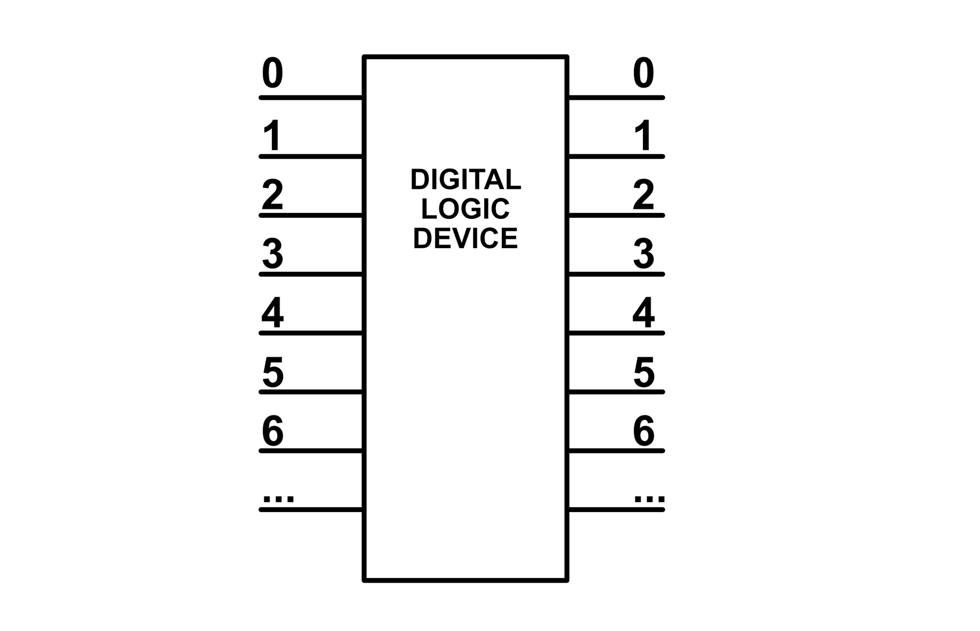
In the devices we've explored, the outputs depend only on the current value of the inputs and the signals are propagated from the inputs to the outputs as quickly as physics permits. This is called combinational logic.
Propagation Delay of Combinational Logic
Even though combinational logic devices intend for the output to instantly change according to the input, there is always a propagation delay, typically proportional to the complexity of the device. Logic device propagation delays must be managed to ensure they are not too long.
Flip-flops are different. Flip-flops are logic elements designed so that their output is determined by both current and past inputs. This type of logic is called sequential logic. Sequential logic is critical for memory and pipeline processing.
Don't be too concerned if flip-flops are more difficult to grasp conceptually than other fundamental logic devices, this is perfectly normal. Their functionality will become clearer with repeated study and thoughtful contemplation.
Set/Reset Flip-Flop
The most basic flip-flop is called a Set/Reset Flip-Flop, or SR Flip-Flop for short. This device is made from two NAND gates, and unlike previous devices we've constructed, the outputs of each NAND gate is plugged into one of the other NAND gate's inputs. This configuration is called feedback.
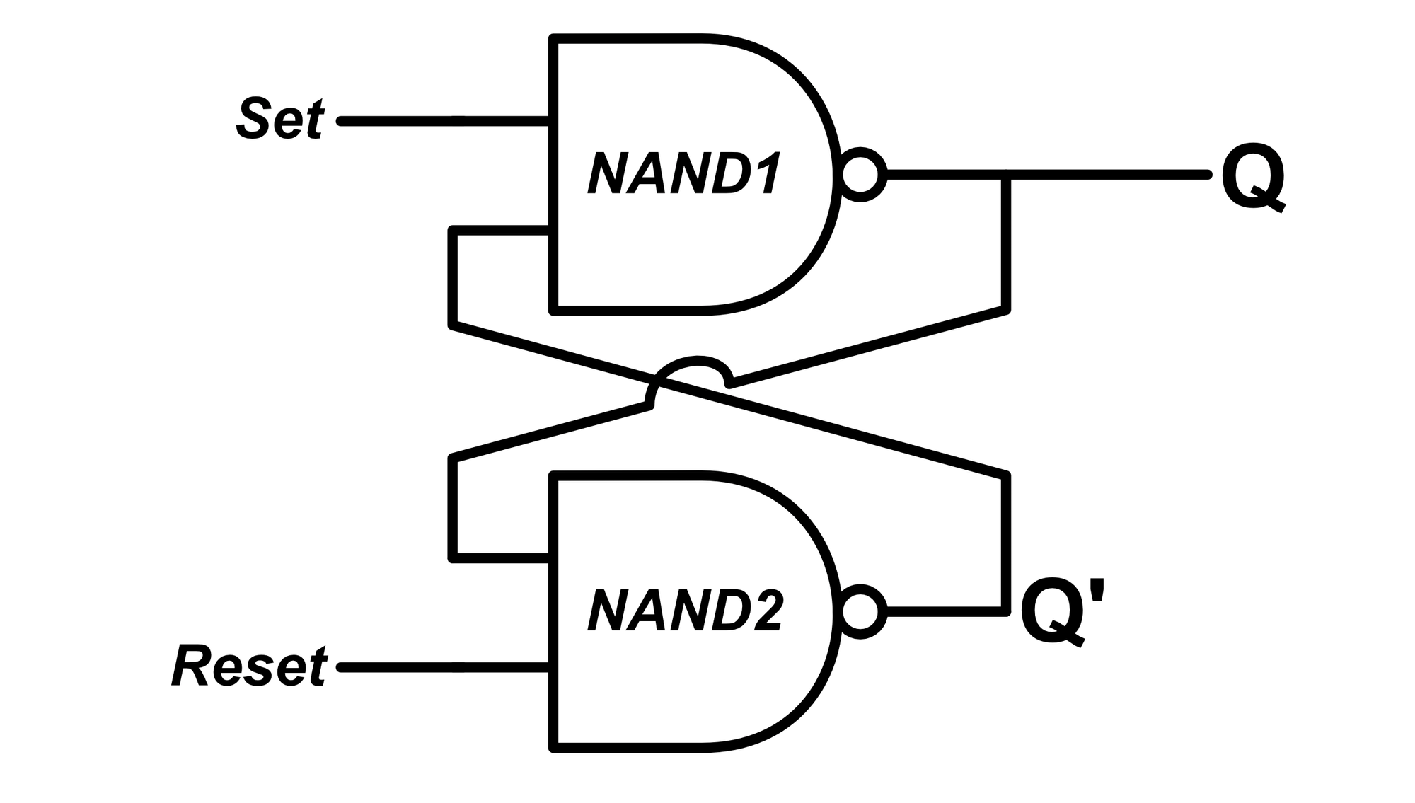
The device has two inputs, SET and RESET. The device has one output, Q. It also has an internal signal called Q'. The objective of this device is to hold a constant logic level at the output Q even if the inputs change.
Maintaining the Status Quo
Suppose that the value of all signals at a moment in time is given by the below table:
| Set | Reset | Q | Q' |
|---|---|---|---|
| 1 | 1 | 1 | 0 |
- Because Q' is 0 and SET is 1, the NAND1 gate outputs 1 so output Q remains 1.
- Because Q is 1 and RESET is 1, the NAND2 gate outputs 0 so Q' remains 0.
As long as we keep SET and RESET equal to 1, the value of Q does not change.
Now, let's consider the case where the values of Q and Q' are flipped:
| Set | Reset | Q | Q' |
|---|---|---|---|
| 1 | 1 | 0 | 1 |
- Because Q' is 1 and SET is 1, the NAND1 gate outputs 0 so output Q remains 0.
- Because Q is 0 and RESET is 1, the NAND2 gate outputs 1 so Q' remains 1.
As long as we keep SET and RESET equal to 1, the value of Q does not change.
The Set Signal
Suppose that the value of all signals at a moment in time is given by the below table:
| Set | Reset | Q | Q' |
|---|---|---|---|
| 0 | 1 | 0 | 1 |
At the first instant in time, the below two events occur:
- Because Q' is 1 and SET is 0, the NAND1 gate outputs 1 so output Q turns to 1 at the start of the next time step.
- Because Q is 0 and RESET is 1, the NAND1 gate outputs 1 so Q' remains 1.
At the next instant in time, the below two events occur:
- Because Q' is 1 and SET is 0, the NAND1 gate outputs 1 so output Q remains 1.
- Because Q is 1 and RESET is 1, the NAND1 gate outputs 0 so Q' turns to 0 at the start of the next time step.
At the next instant in time, the below two events occur:
- Because Q' is 0 and SET is 0, the NAND1 gate outputs 1 so output Q remains 1.
- Because Q is 1 and RESET is 1, the NAND1 gate outputs 0 so Q' remains 0.
At this point, the gate outputs continue to be stable until we change the input signals. Remember from the previous section that if both SET and RESET inputs are 1, the output also doesn't change.
The effective result of this process is that we have set the signal Q to a value of 1. Though we did not intend for it, the internal signal Q' has also flipped from 1 to 0. We describe the initial states Q and Q' as Qi and Q'i and the final states as Qf and Q'f.
| Qi | Q'i | Qf | Q'f |
|---|---|---|---|
| 0 | 1 | 1 | 0 |
Above, we've shown the initial and final signals, but we could have also shown each intermediate signal from the initial instant 0 to the final stable time 3.
| Q0 | Q'0 | Q1 | Q'1 | Q2 | Q'2 | Q3 | Q'3 |
|---|---|---|---|---|---|---|---|
| 0 | 1 | 1 | 1 | 1 | 0 | 1 | 0 |
We can compress this entire process into a logic sequence diagram, shown below.

The inputs and initial signals, Q0 and Q'0 are shown. The resulting signals Q1 to Q4 and Q'1 to Q'4 are then sequenced. The decision to limit the number of sequenced steps to 4 is because useful signals are stable by this point.
Using the same method, we can calculate the logic sequence for SET = 0 and RESET = 1 when the initial states Q0 and Q'0 are reversed. We find in this situation that the output Q remains unchanged (it is already set to 1).
We can also add the earlier do nothing sequences from the previous section.

The Reset Signal
The set signal was performed by assigning SET = 0 and RESET = 1.
The reset signal is performed by assigning SET = 1 and RESET = 0. Like previous signal types, we can create a table:

This table describes all the useful sequences for our device. We can either set Q to 1, reset Q to 0, or let the device do nothing and maintain whatever its current state is.
The Full Logic Table
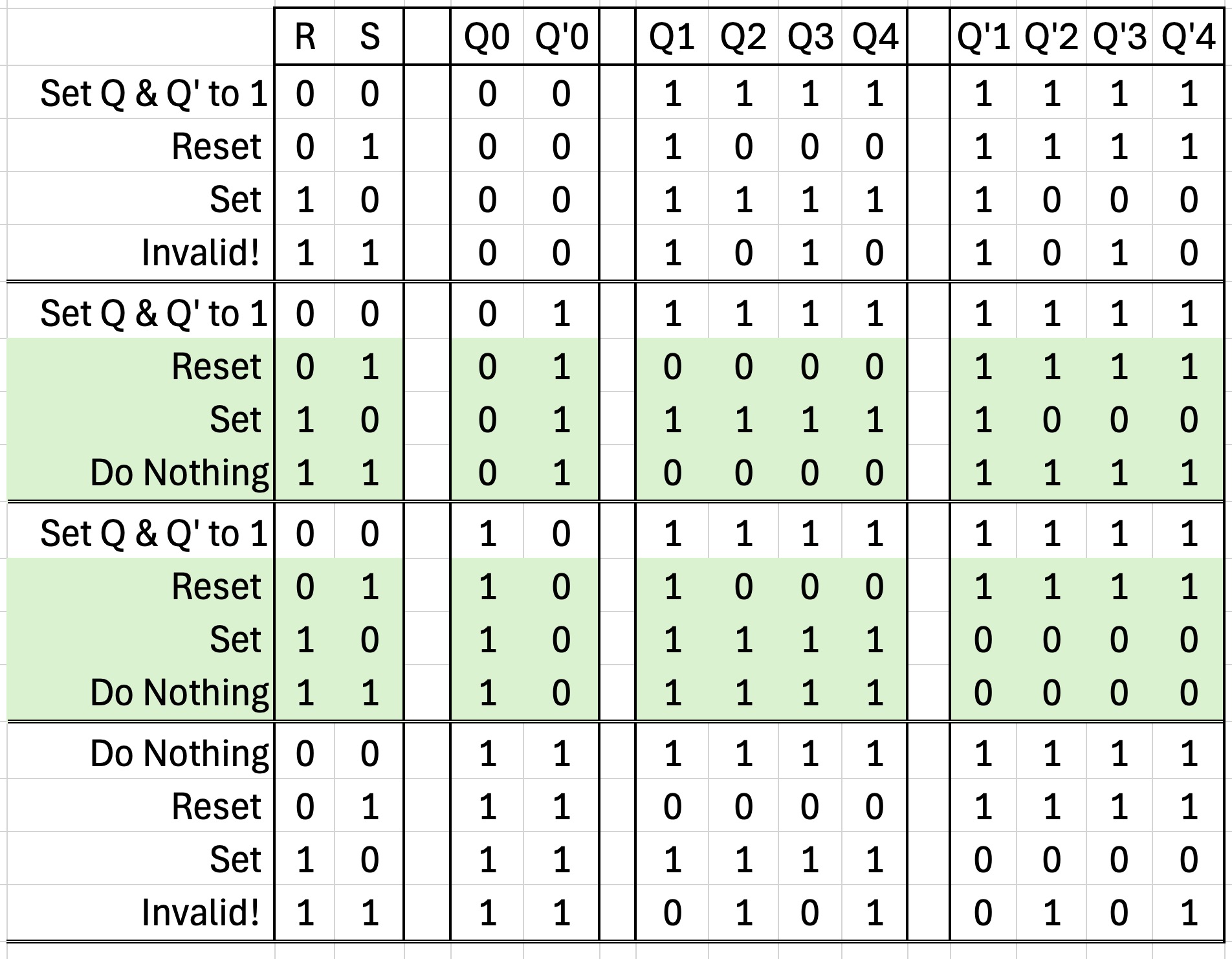
Even though the table in figure 5 contains the full set of useful sequences, it doesn't contain all the possibilities.
- What happens if Q, Q', Reset, and Set are all zero because we've just barely turned the device on?
- What happens if Q and Q' are zero but Reset and Set are both 1?
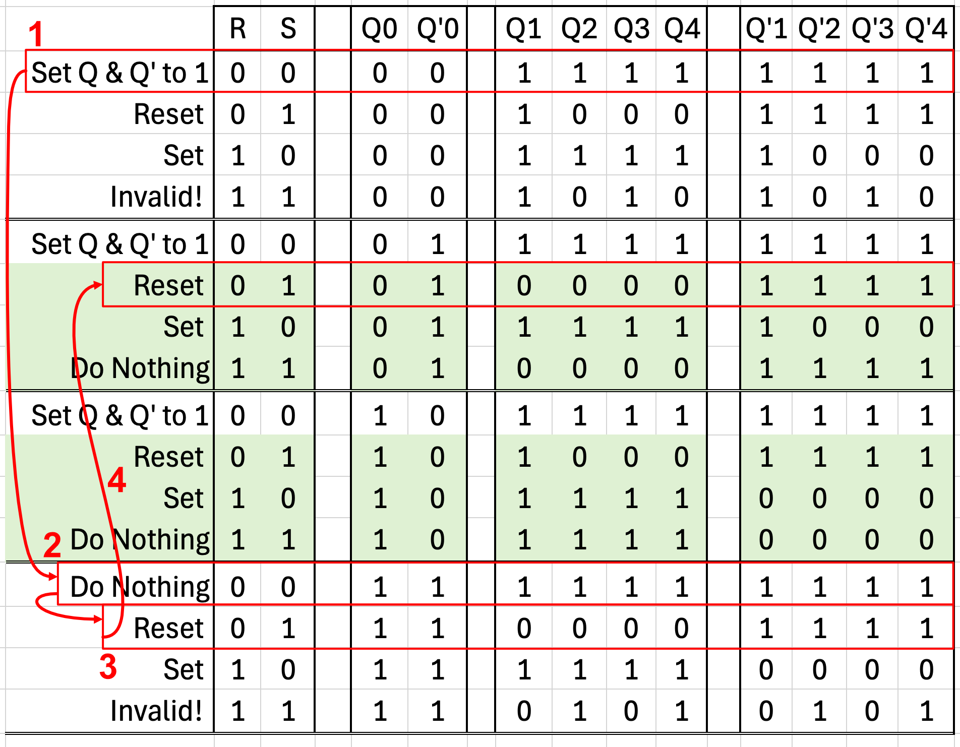
All of these questions and more are answered with the full logic diagram, shown below. The useful sequences are highlighted in green:
Initialization
Because the logic level of all device gates is typically zero when it is turned on for the first time, we need a means to get the device into a known good state within our green zone. This is accomplished simply by applying the reset signal until Q0 becomes 0 and Q'0 becomes 1. At this point, the device is now ready for use.
Invalid Sequences
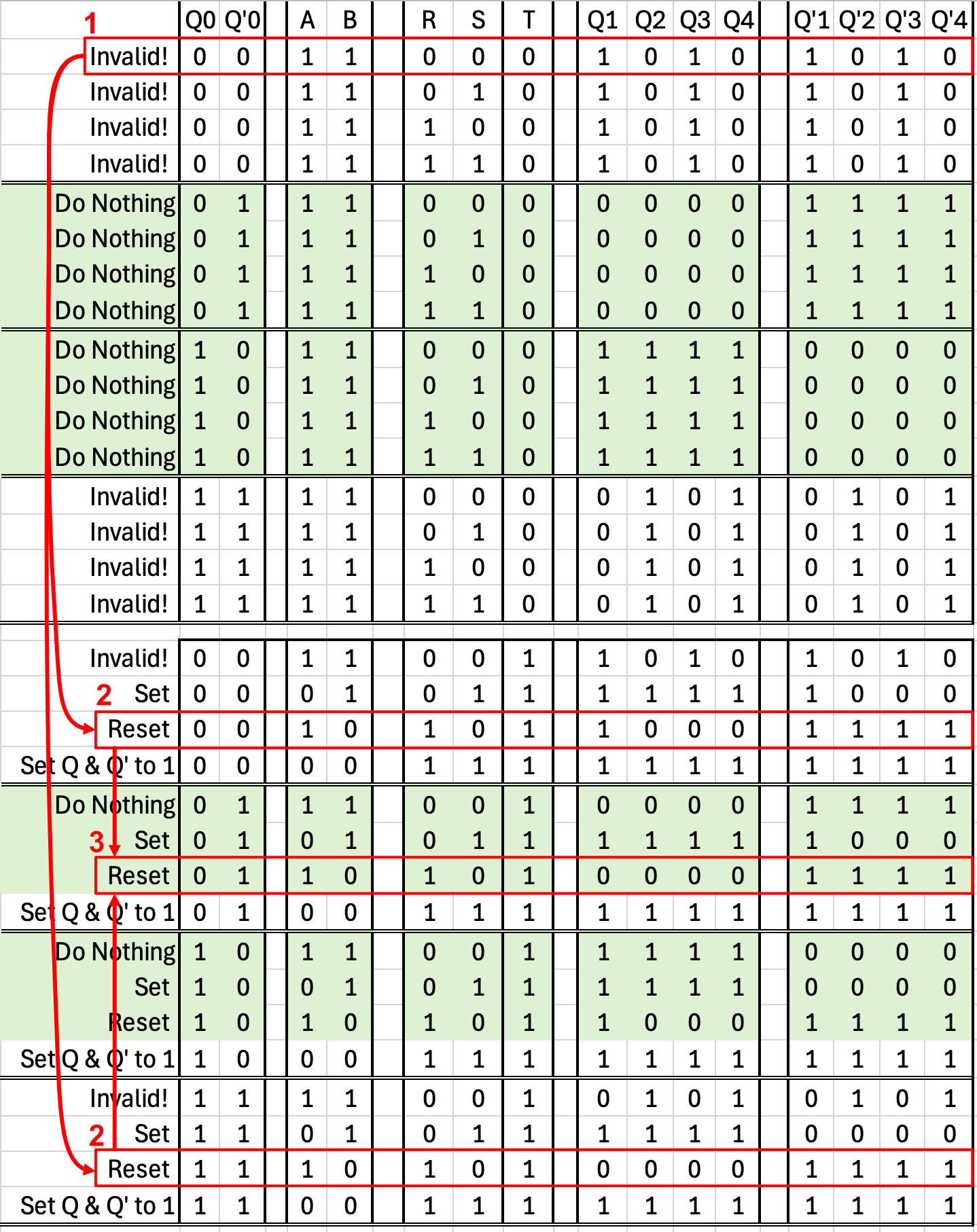
You may have noticed the rows labeled "Invalid!", shown below:
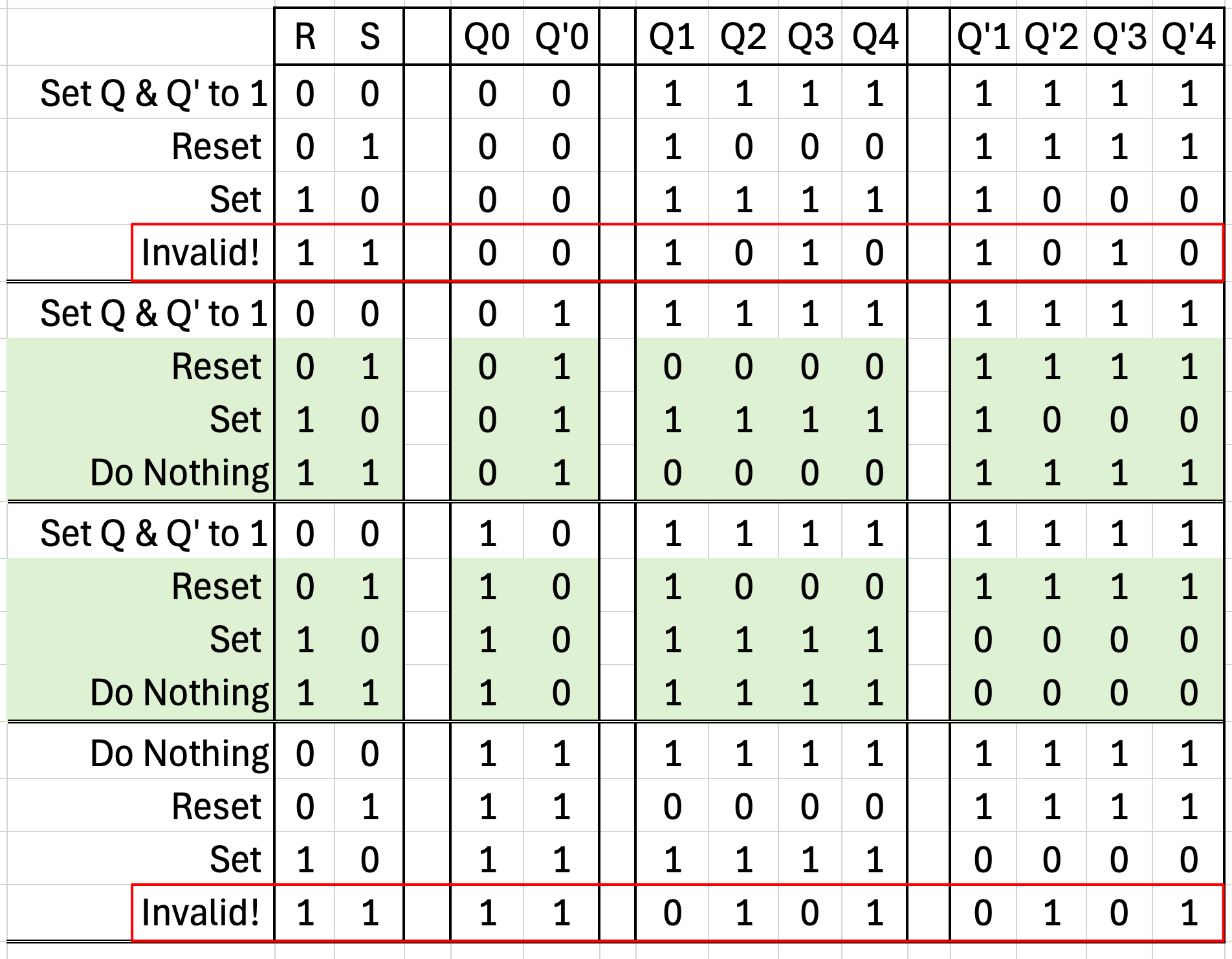
If we look at the progression sequence for these invalid sequences, Q and Q' have the same value and oscillate between 0 and 1. This oscillation will occur as fast as the gates allow it to occur per their underlying physics.
Unless we are looking for rapid chaotic oscillation, we shouldn't put our device into this state. If we accidentally did so, we can apply either a RESET or SET signal to get it out and back into the normal operating sequences (shown in green).
Triggered Set/Reset Flip-Flop
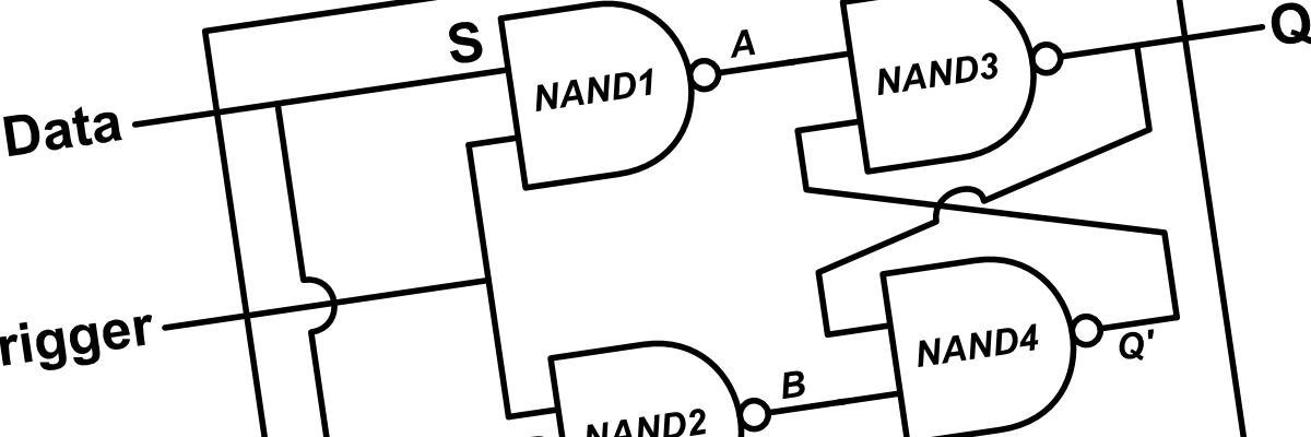
Rather than having the flip-flop change states whenever we change the inputs, we may want to only have the flip-flop change states when we set another input, TRIGGER, to 1. We do this by adding another pair of NAND gates.
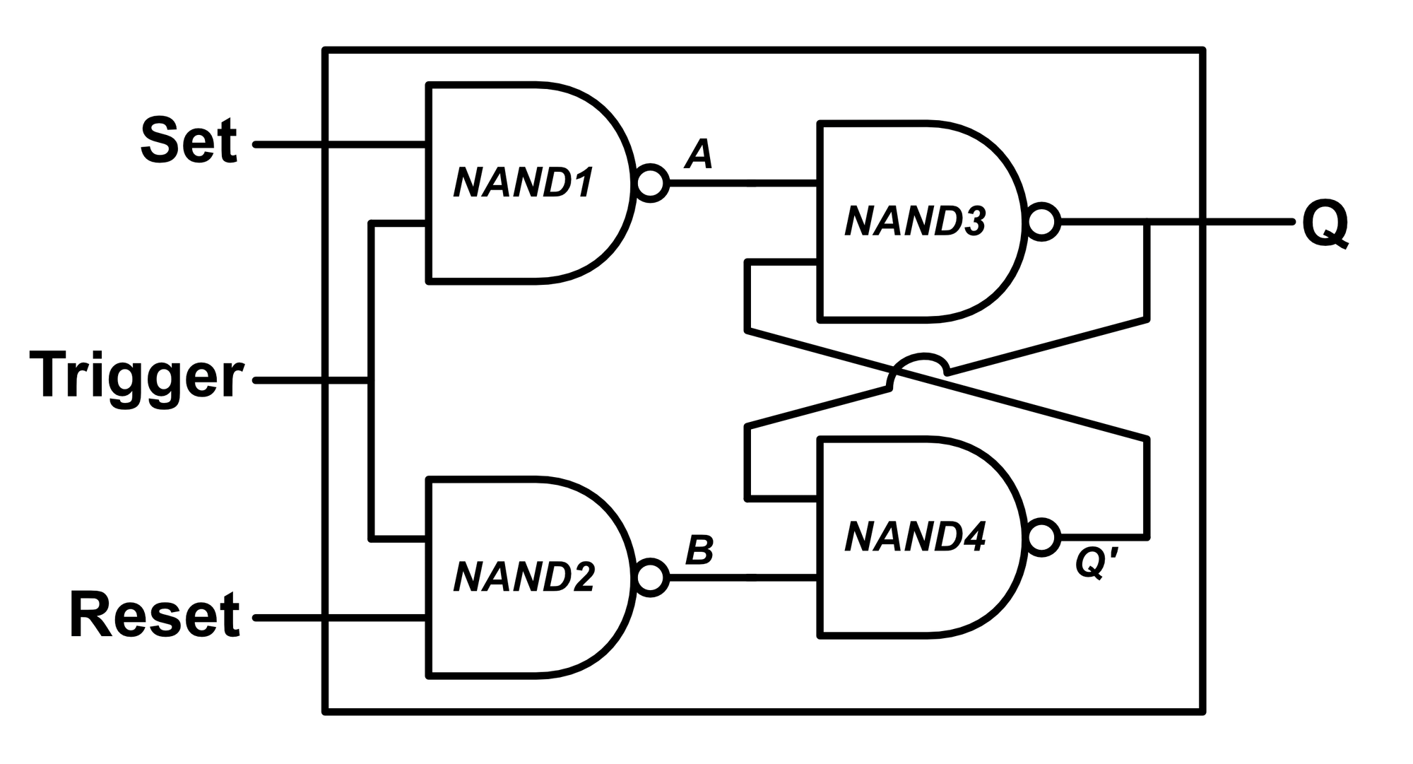
The complete logic diagram for this device is shown below:
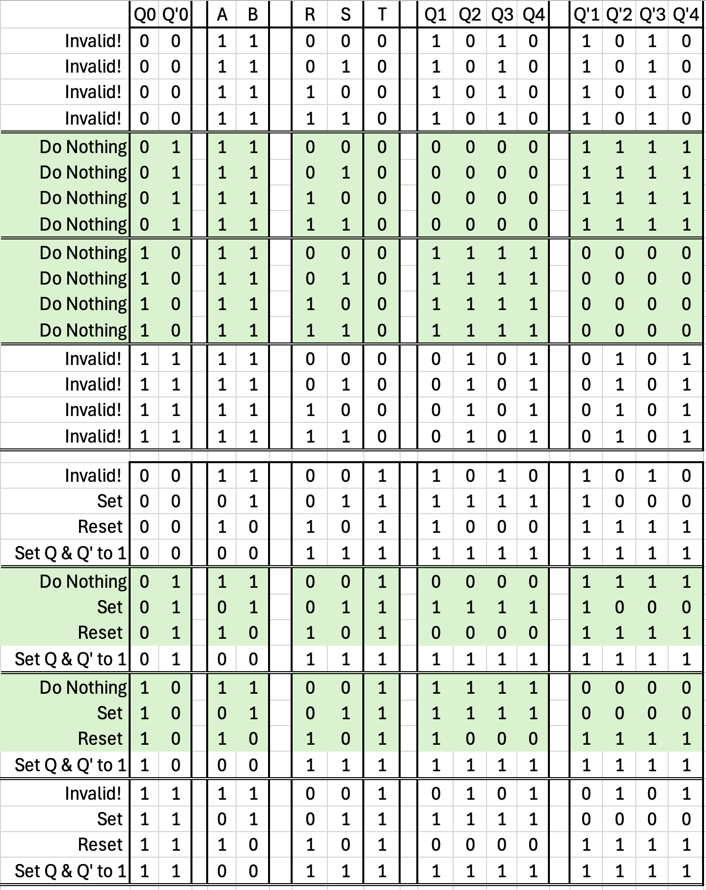
This may appear intimidating, but if we only pay attention to the actual green operating part of the diagram, things become much clearer:
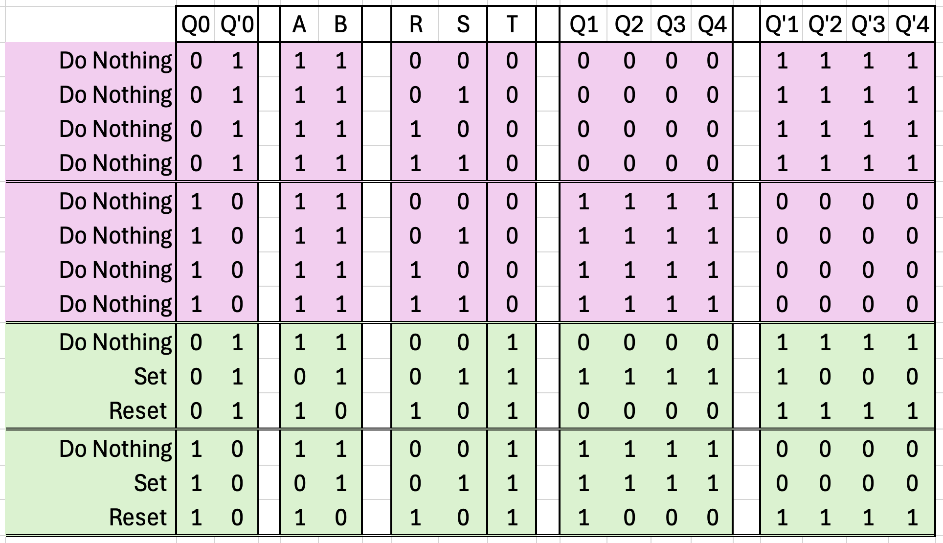
As we can see, if the trigger input is 0, the output states remain unmodified. If the trigger input is 1, the device behaves almost exactly like our original SR Flip-Flop, except to set the output high, SET is assigned 1 instead of 0. To reset the output low, RESET is assigned 1 instead of 0.
Initialization
When we initially turn on the trigger flip-flop, it actually initializes into that horrible oscillating sequence. We can get it back into a stable operating sequence by sending the reset signal with the trigger high.
The D-type Flip-Flop
Dealing with both the SET and RESET lines is a pain. What we'd really like is a single DATA line and to be able to set the flip-flop high if the DATA line is high and low if the DATA line is low. This is done by connecting the SET line to the RESET line through a NOT gate.
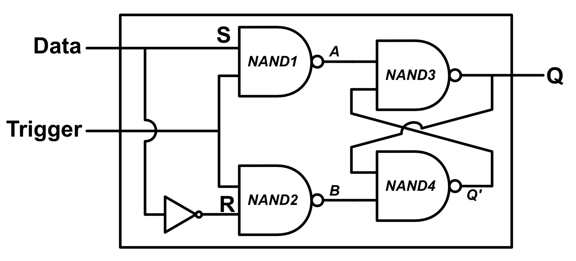
At last, we've finally arrived at the D-type Flip-Flop, arguably the most widely used flip-flop in all of computer engineering.
Because of the NOT gate between S and R, there are no valid sequences where SET and RESET have the same logic value. We can cross these out from the Triggered Set/Reset Flip Flop Logic Table:
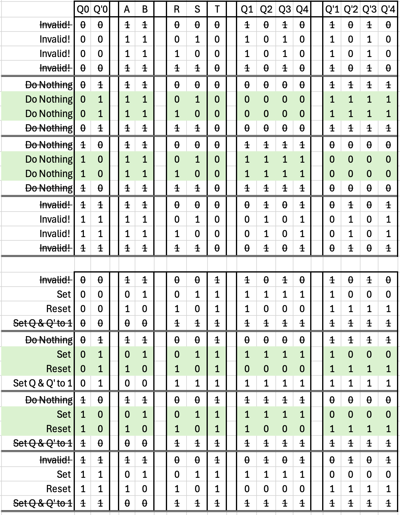
Since they are crossed out, we might as well delete them to make the table smaller:
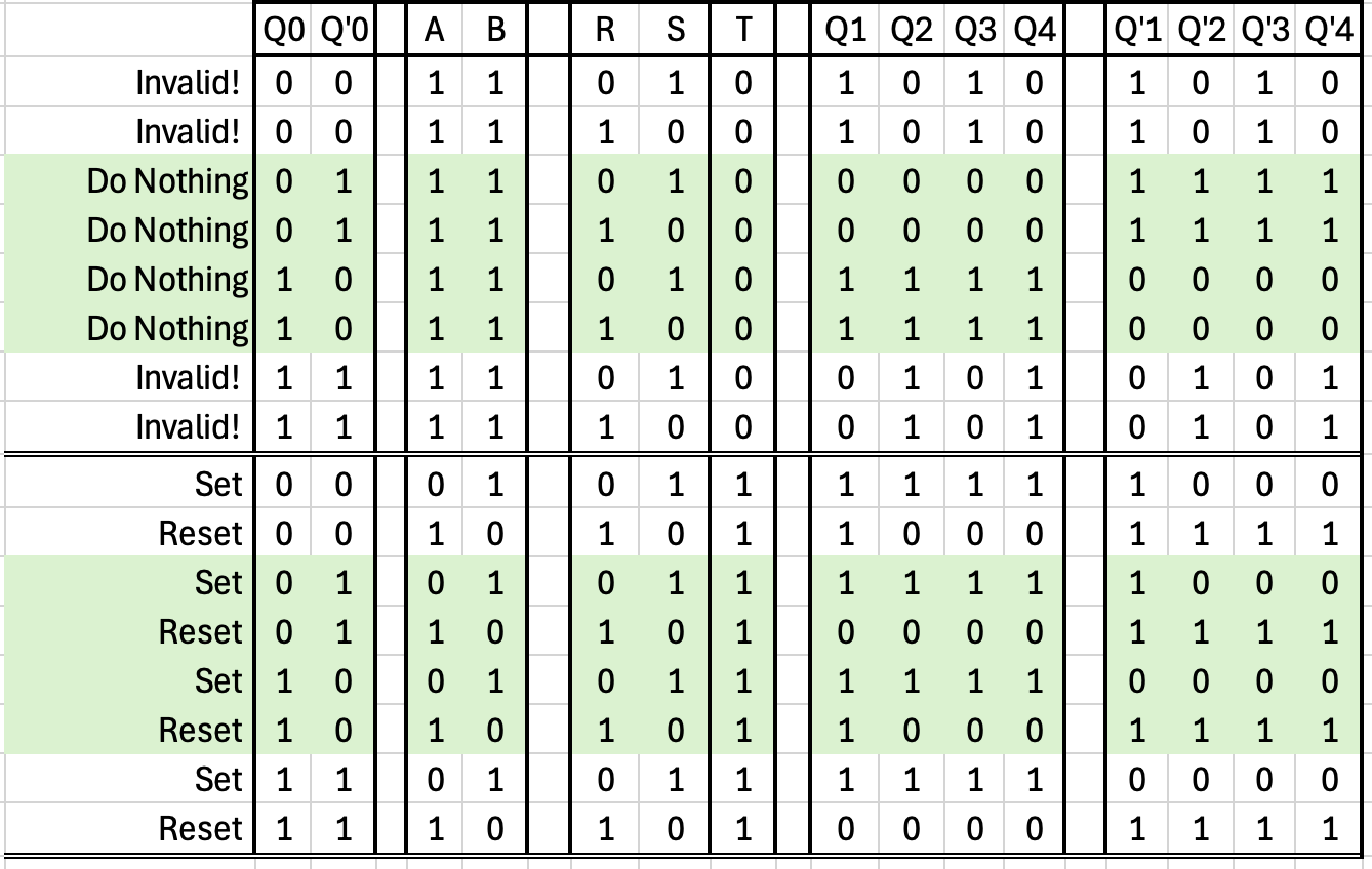
If we only use the device as prescribed (applying the reset signal after turning it on), we remove the possibility of putting the device into a state where Q and Q' are the same, therefore we can also remove those rows from the table (and recolor the green rows white):
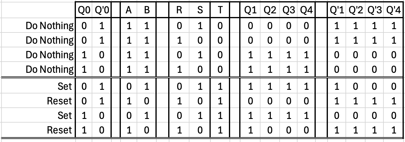
Since Data is connected to S, we can rename S to D:
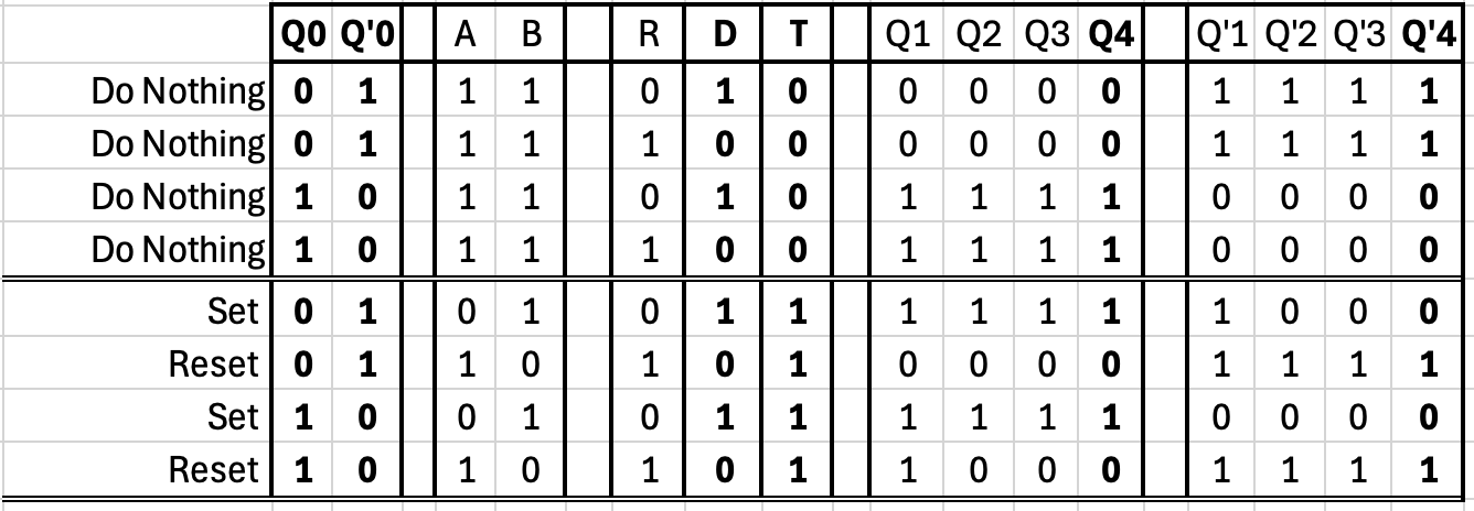
If we treat the D-type Flip Flop as an abstract discrete logic device, we obtain the below diagram and logic table.
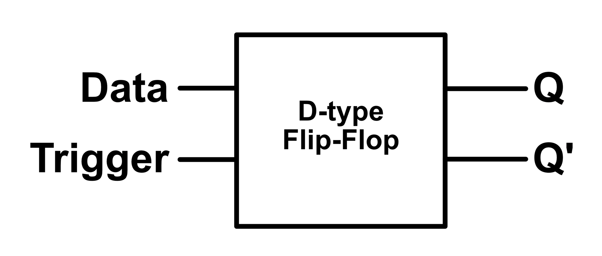
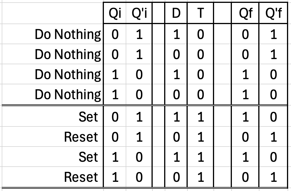
Previously, we treated Q' as an internal signal, but Q' is often also output to save the designer a NOT gate in case they want Q' and not Q.
