Logic Gates
Prerequisites Required- Logic Switches
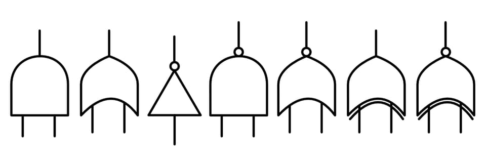
The most fundamental component of a computer is a logic switch, however, computer engineers don't design a computer by arranging raw logic switches. Instead, they arrange logic switches into larger abstract logic components. Those larger components then get arranged into even larger logic components. With enough stacked layers, you eventually get modern CPUs, graphics cards, arithmetic units, and more. Logic design is like the ultimate building toy! The first layer of logical building block above logic switches is the logic gate. There are seven main types of logic gate; AND, OR, NOT, NAND, NOR, XOR, XNOR.
Logic Switch Review
Let's consider a high side logic switch with the input $A$ connected to logic high ($1$) and $B$ left as an input. When $B$ is low, the switch is open and the pull-down resistor causes the output to be logic low ($0$). When $B$ is high, the switch is closed and the output is logic high ($1$). The switch diagram and its corresponding logic table are shown below:
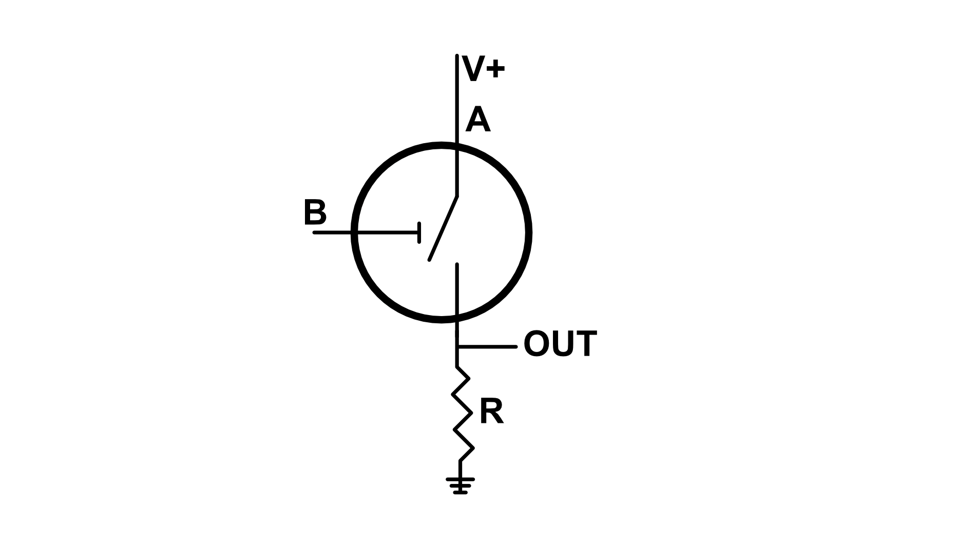
| A | B | Output |
|---|---|---|
| 1 | 0 | 0 |
| 1 | 1 | 1 |
The AND Gate
If we stack another switch on top of our existing high side switch in series, and label the control inputs to each switch as $A$ and $B$, we obtain an AND gate.
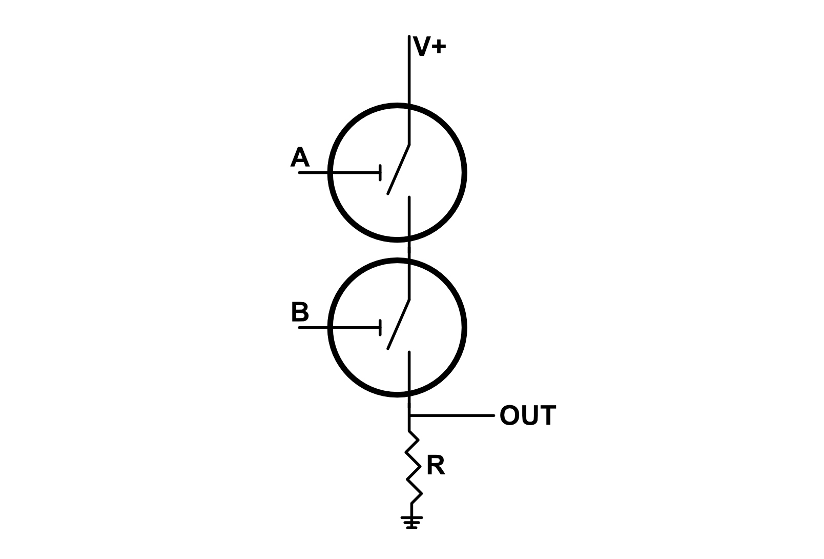
If either $A$ or $B$ are logic low ($0$), one of the switches will remain open and the output will be pulled to ground ($0$). If $a$ AND $b$ are logic high ($1$), the output will be logic high. This is why this configuration of switches is called an AND gate. The logic table for an AND gate is shown below:
| A | B | Output |
|---|---|---|
| 0 | 0 | 0 |
| 1 | 0 | 0 |
| 0 | 1 | 0 |
| 1 | 1 | 1 |
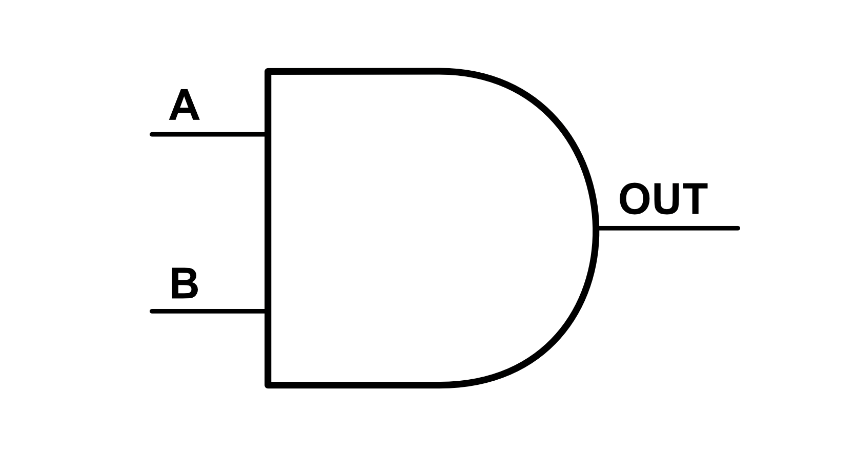
Since drawing switches is cumbersome, the AND gate has a special universal symbol:
The OR Gate
If we connect a switch next to our original high side switch in parallel, and label the control inputs to each switch as $A$ and $B$, we obtain an OR gate.
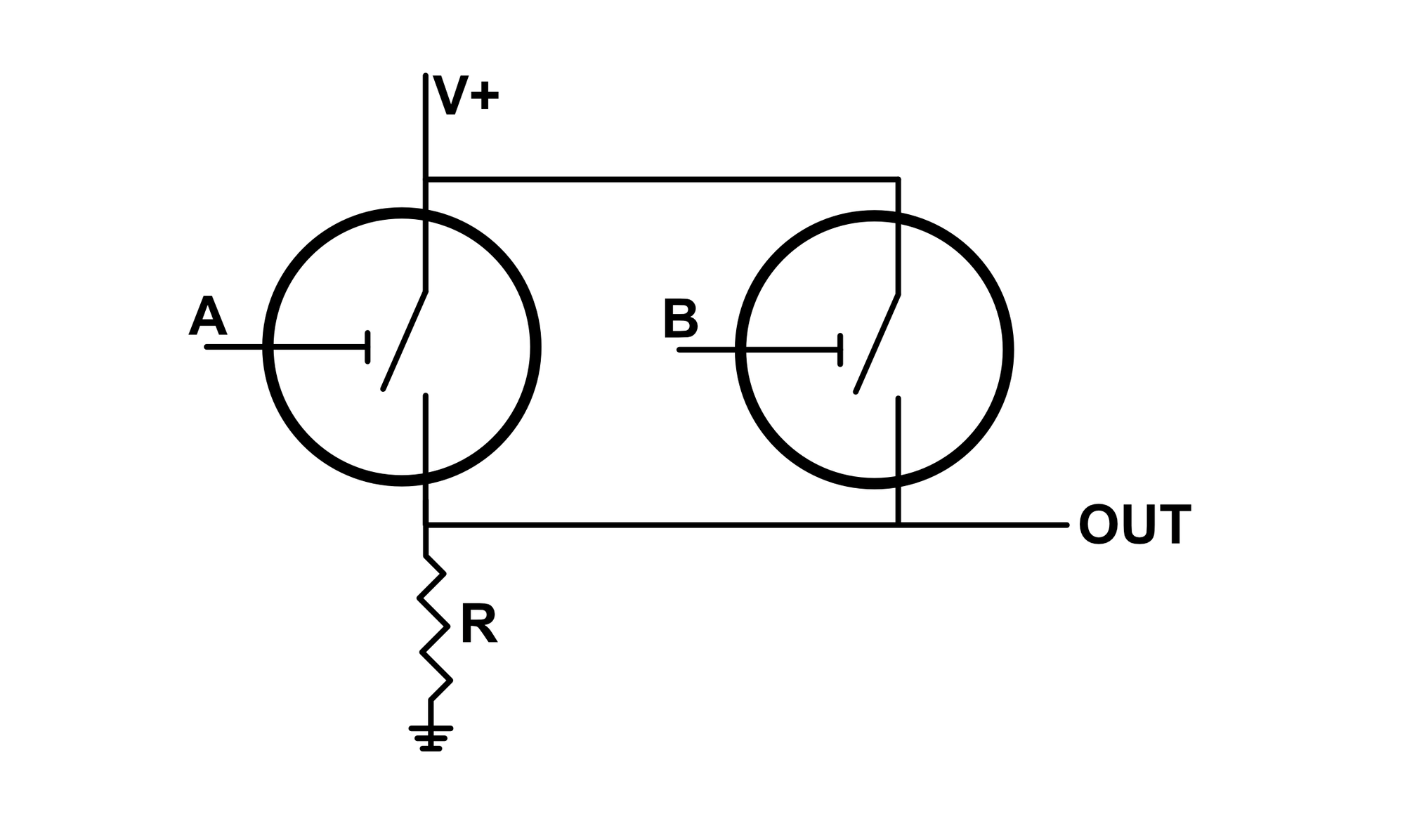
If either $A$ OR $B$ are logic high ($1$), one of the switches will close and the output will be logic high ($1$). This also happens if both switches are high. The logic table for an OR gate is shown below:
| A | B | Output |
|---|---|---|
| 0 | 0 | 0 |
| 1 | 0 | 1 |
| 0 | 1 | 1 |
| 1 | 1 | 1 |
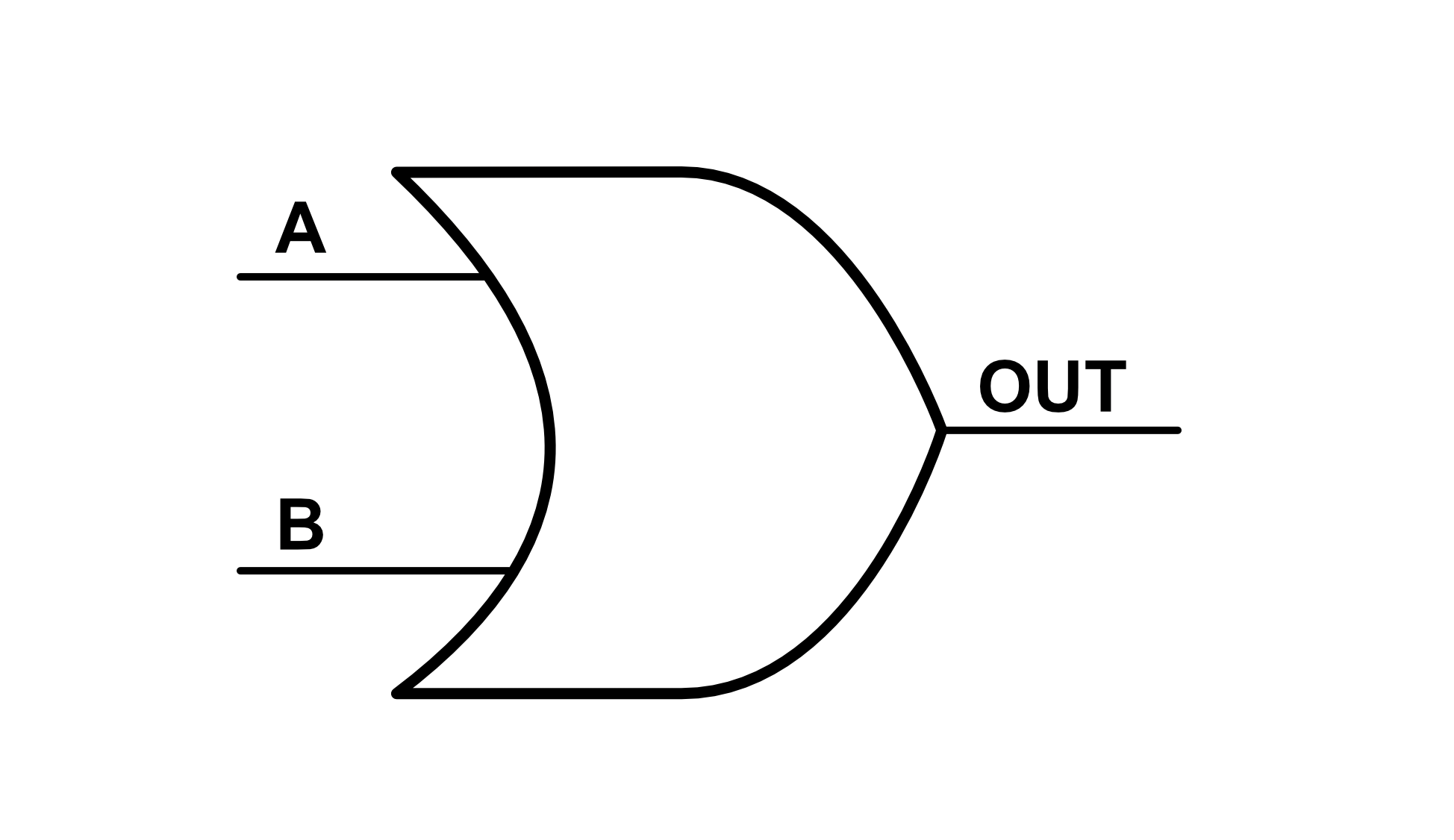
The OR gate also has a special universal symbol:
The NOT Gate
If we connect one end of a switch to ground and the other to a resistor connected to logic high, we obtain a NOT gate.
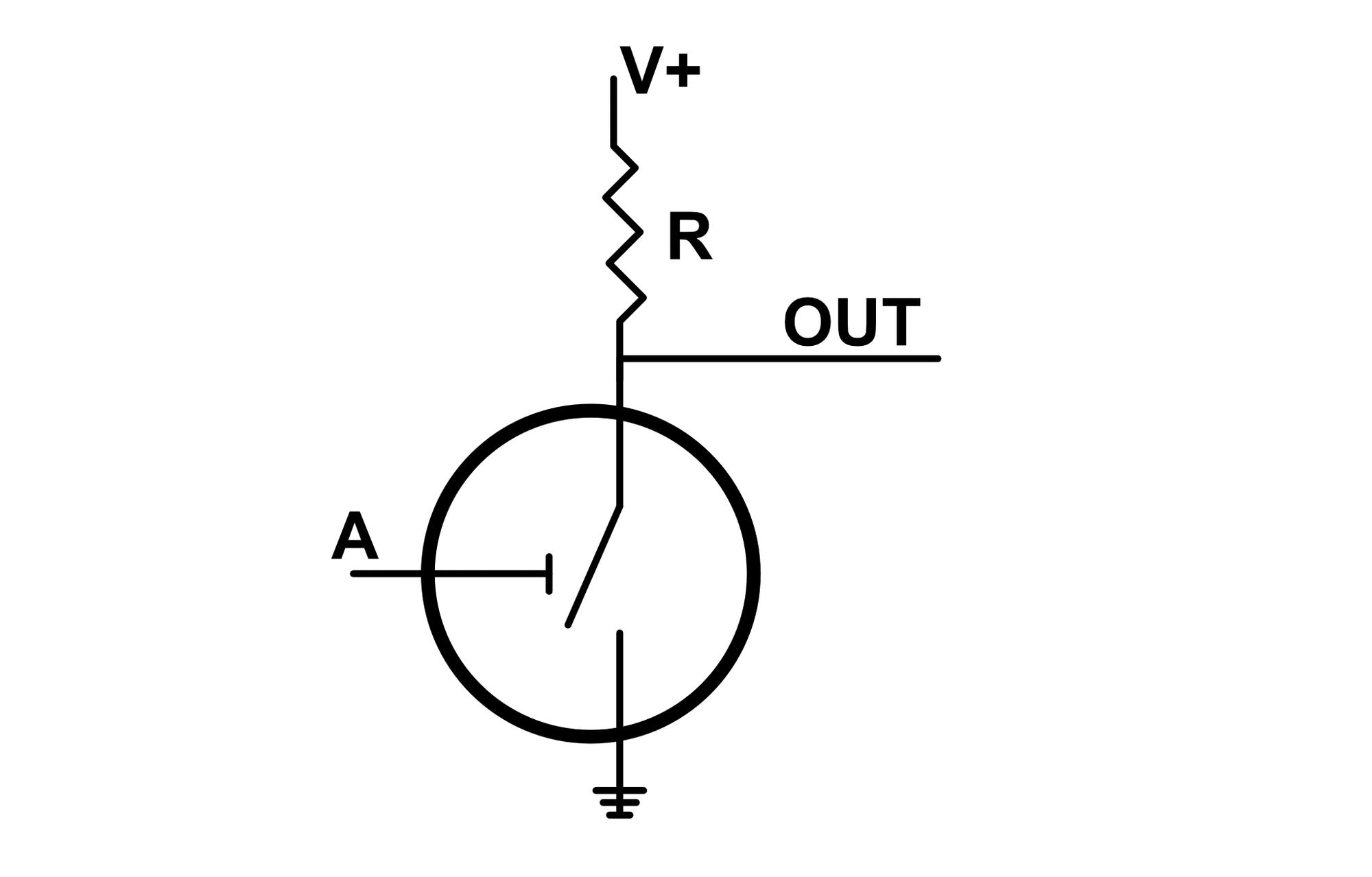
When $A$ is low, the switch is open, so the output is high. When $A$ is high, the switch is closed and the output is pulled low. Because of this, the output of the gate is NOT $A$, it's the opposite of $A$.
| A | Output |
|---|---|
| 0 | 1 |
| 1 | 0 |
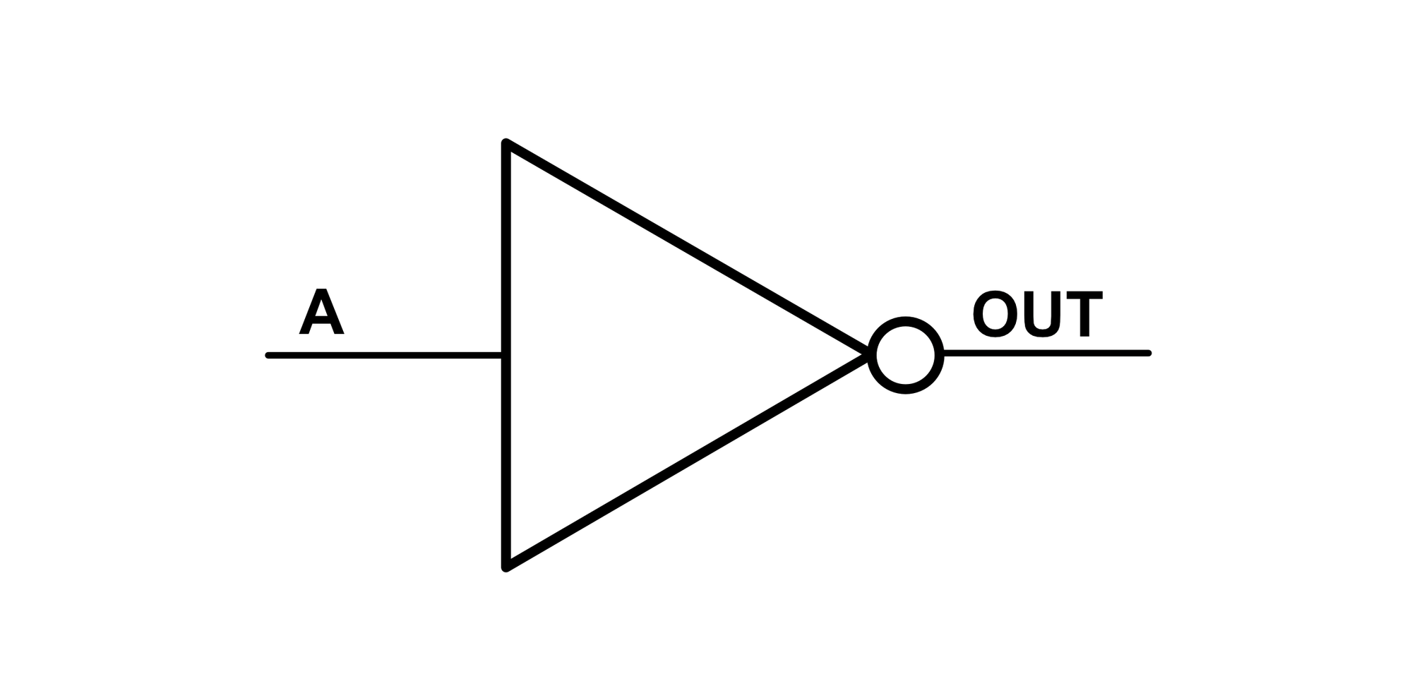
The special symbol for the NOT gate is shown below:
The NAND Gate
If we combine the designs of the AND gate and the NOT gate, we obtain the NAND gate, short for NOT AND.
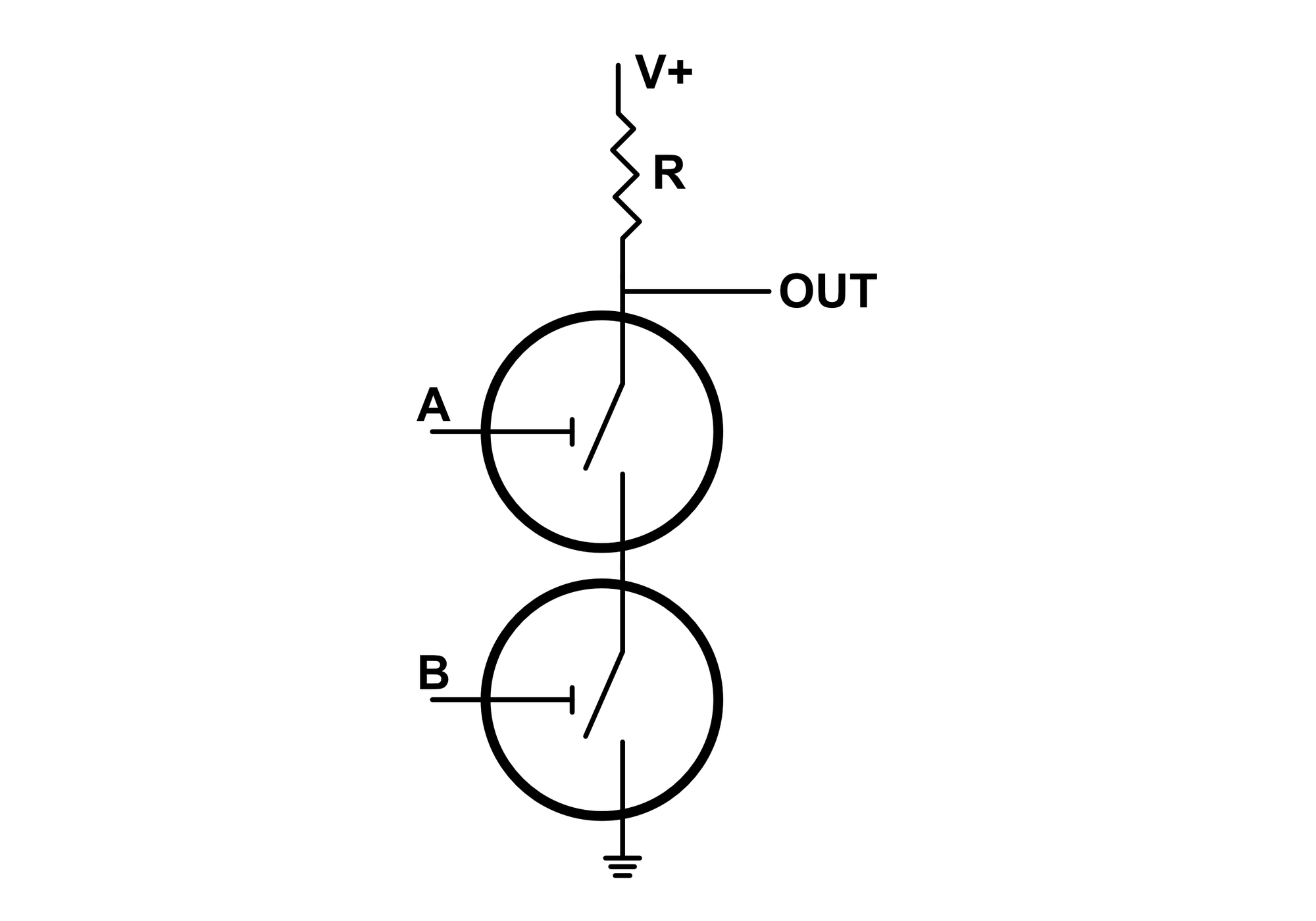
This gate is the exact opposite of the AND gate. If $A$ AND $B$ are logic high, the output is pulled low. Otherwise, the output is high.
| A | B | Output |
|---|---|---|
| 0 | 0 | 1 |
| 1 | 0 | 1 |
| 0 | 1 | 1 |
| 1 | 1 | 0 |
The NAND gate symbol is shown below:
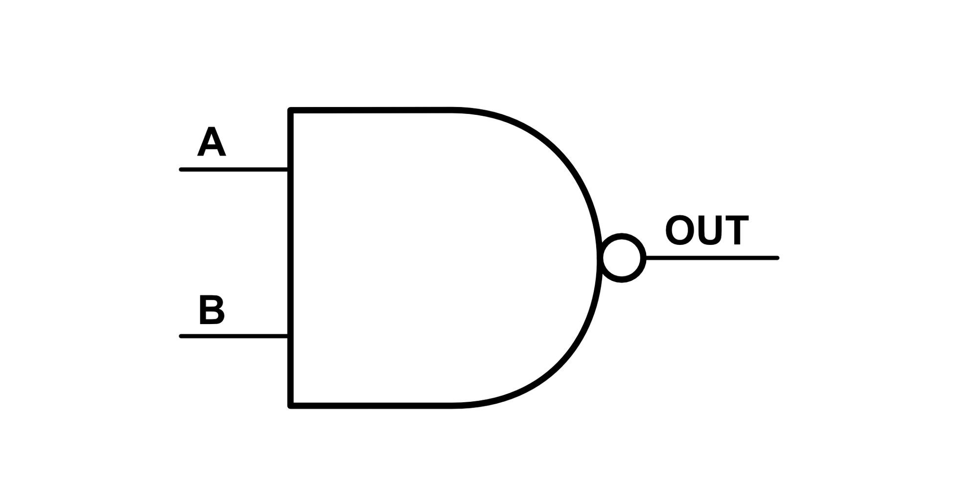
NAND gates are extremely common because they can be arranged to make any other type of gate. This property is called functional completeness. Making other gates out of NAND gates is not the most efficient use of switches, but the fact that it's possible to do so makes NAND gates special. Rather than digressing here, this special property deserves its own article.
The NOR Gate
In a similar manner to the NAND gate, we can combine the NOT and OR gate topology to obtain the NOR gate.
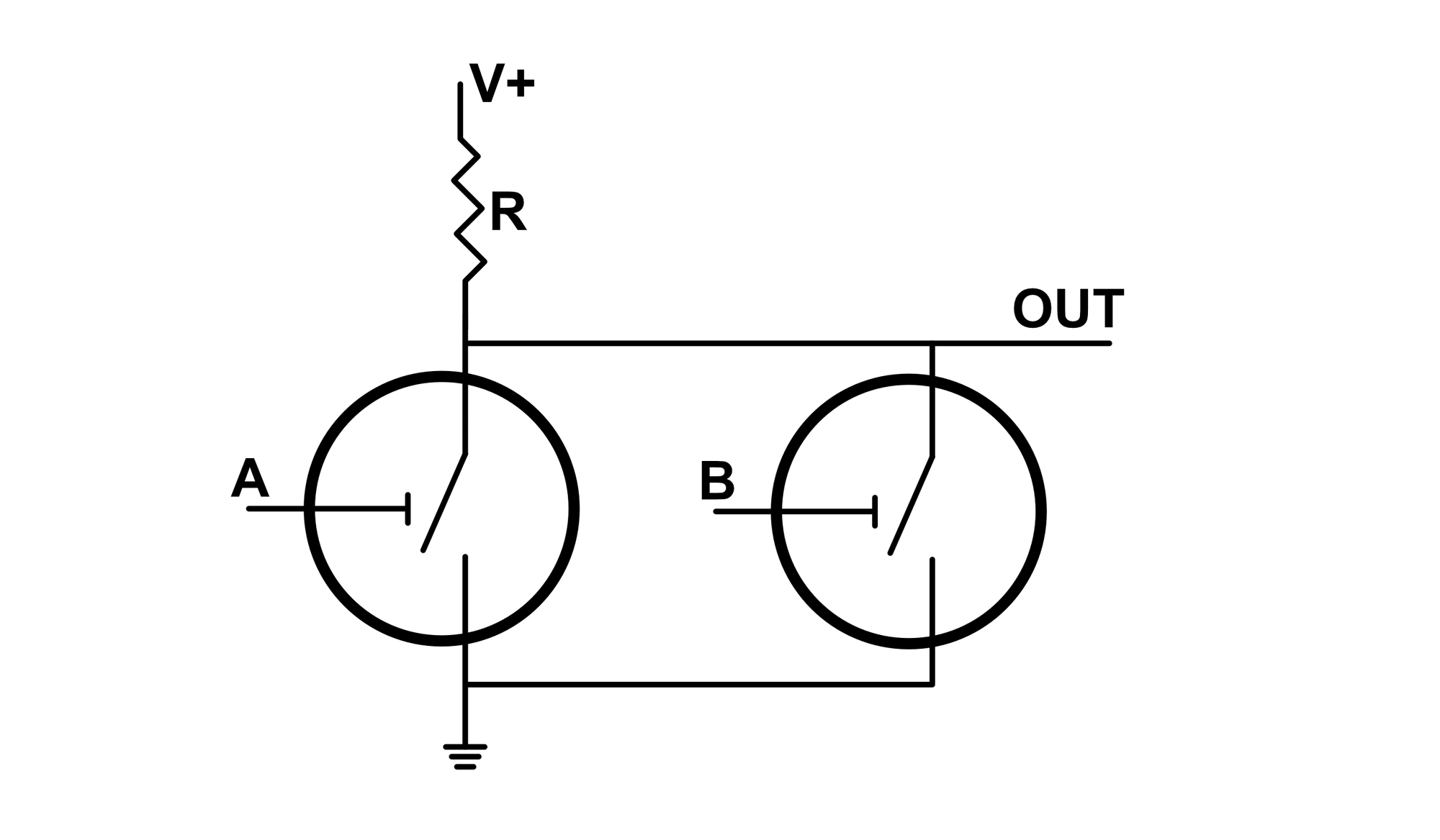
This gate is the exact opposite of the OR gate. If $A$, $B$, or both are low, the output is high, otherwise the output is low.
| A | B | Output |
|---|---|---|
| 0 | 0 | 1 |
| 1 | 0 | 0 |
| 0 | 1 | 0 |
| 1 | 1 | 0 |
The NOR gate symbol is shown below:
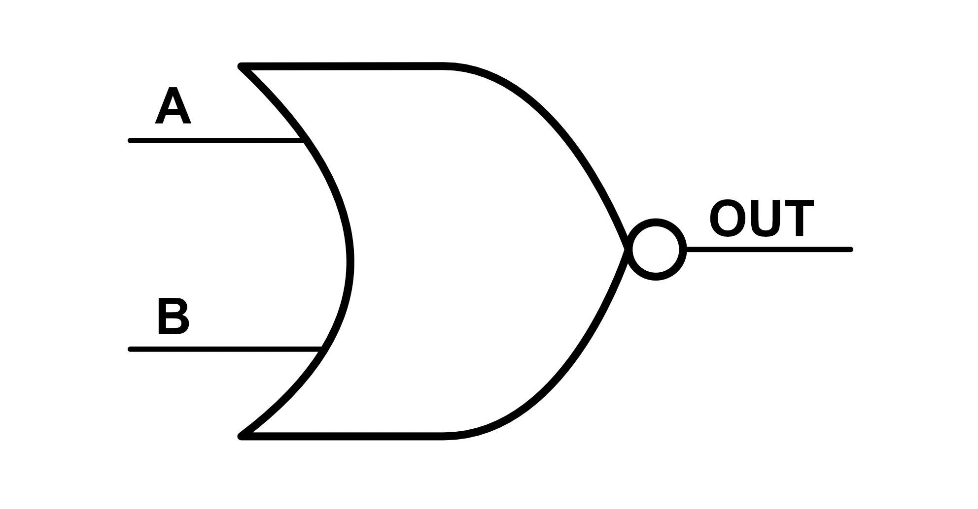
The NOR gate is also functionally complete.
The XOR Gate
The XOR gate is similar to the OR gate, but the output of this gate is only high when EITHER $A$ or $B$ is high, but not both. The logical construction of this gate is very simple. We connect the outputs of parallel OR and NAND gates into an AND gate. This is shown below:
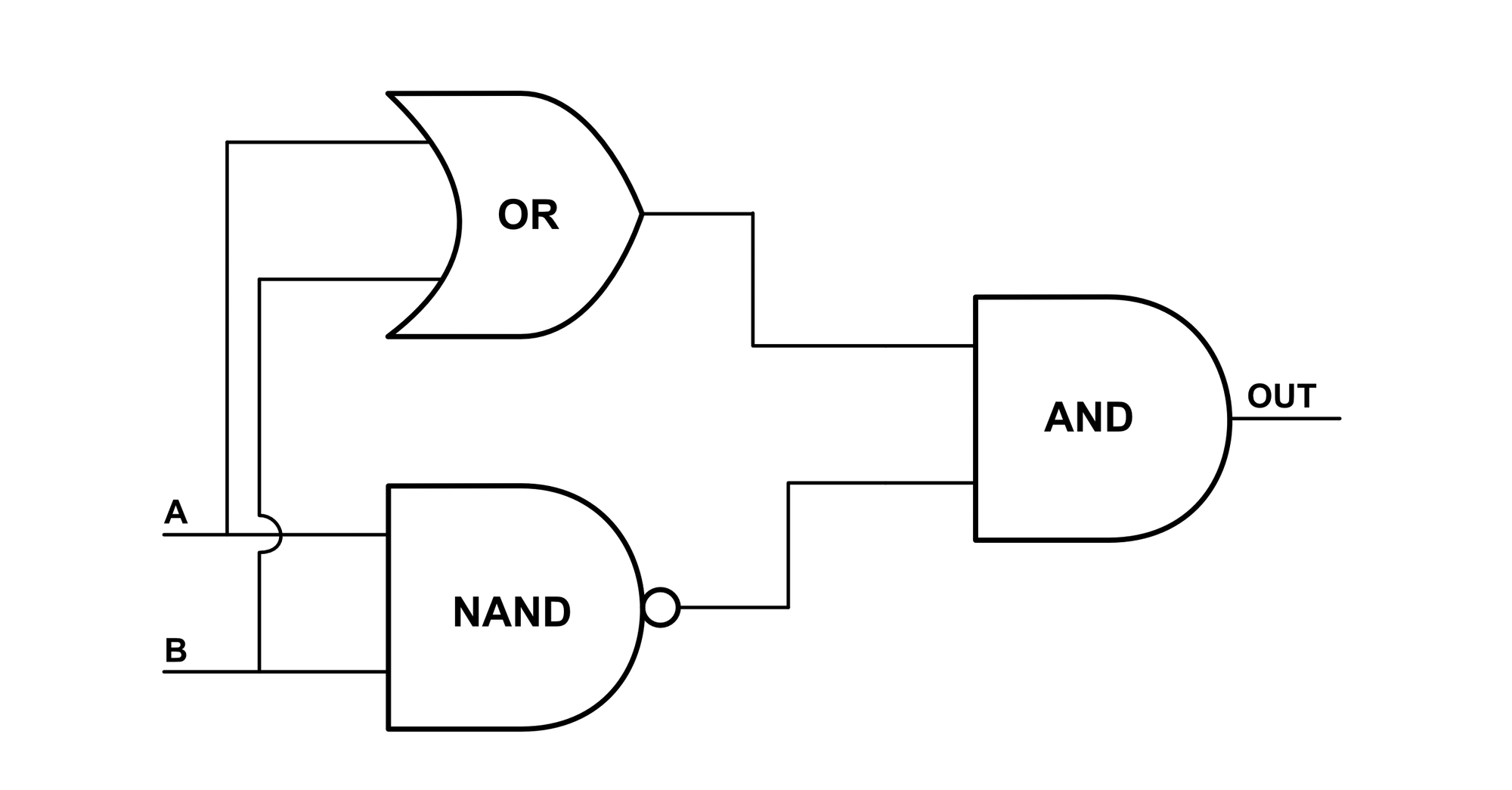
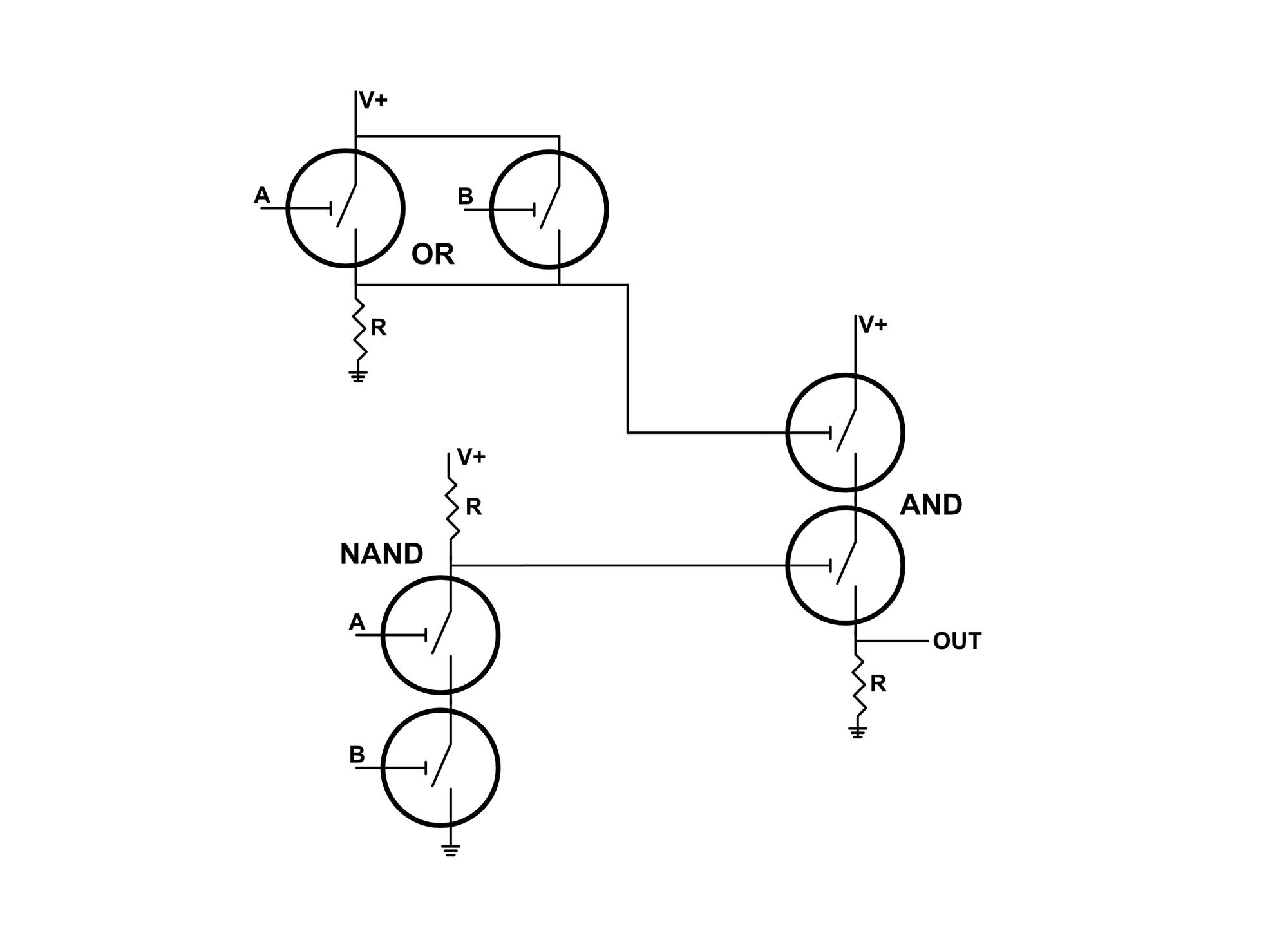
The XOR gate is the first gate that is more difficult to devise from raw switches than from logic gates. We can of course draw the XOR gate using raw switches (an actual hardware implementation would need to be built using switches) but as shown below, we can see how the XOR gate diagram using switches is already starting to become overwhelming.
The XOR logic table is shown below:
| A | B | Output |
|---|---|---|
| 0 | 0 | 0 |
| 1 | 0 | 1 |
| 0 | 1 | 1 |
| 1 | 1 | 0 |
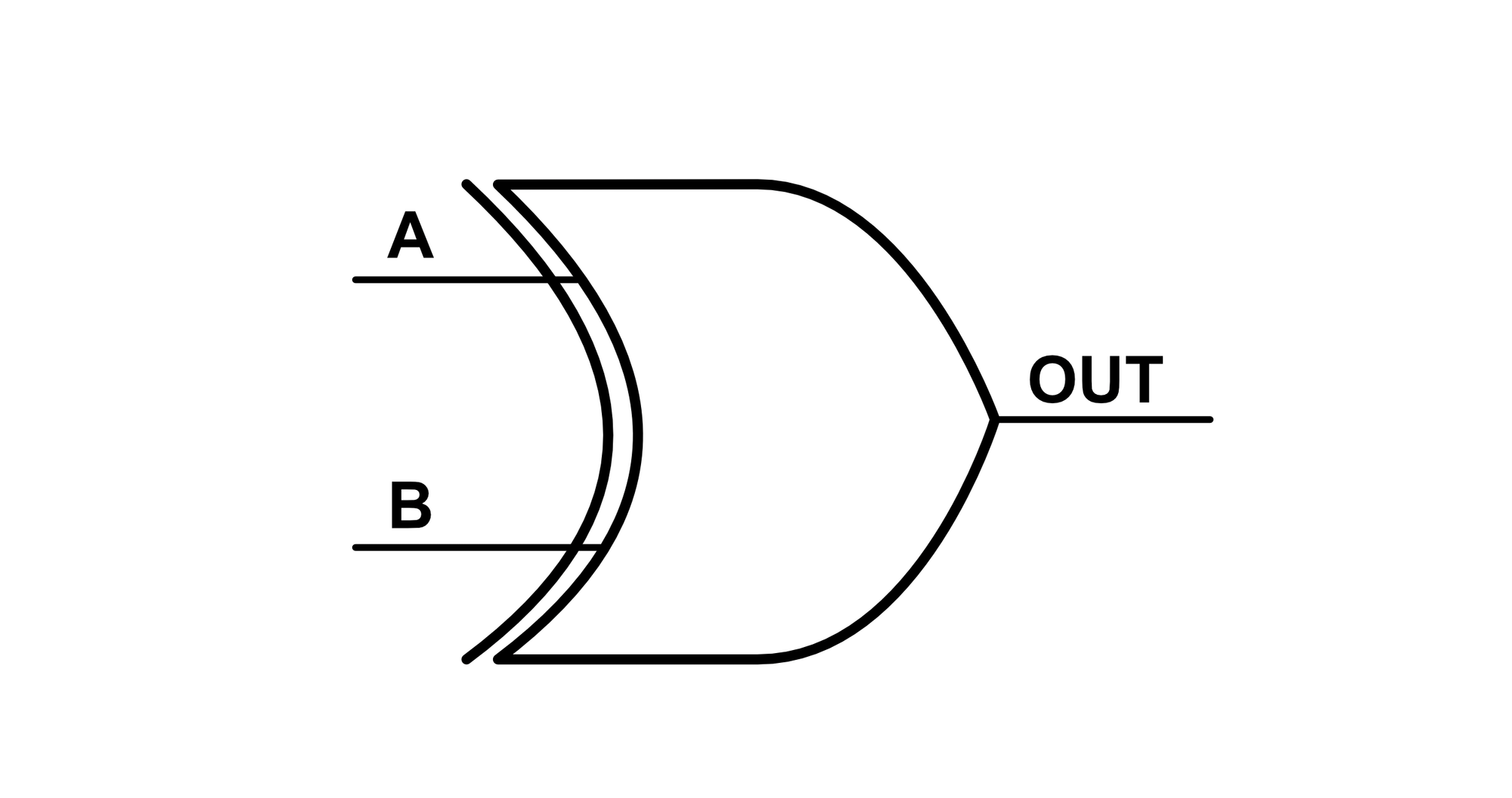
The XOR gate symbol is shown below:
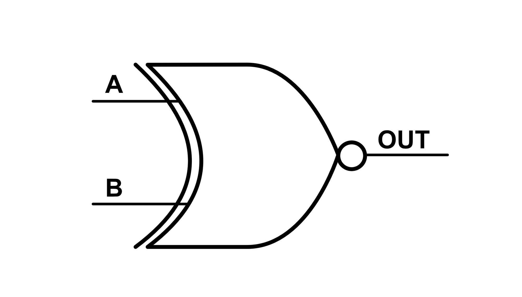
The XNOR Gate
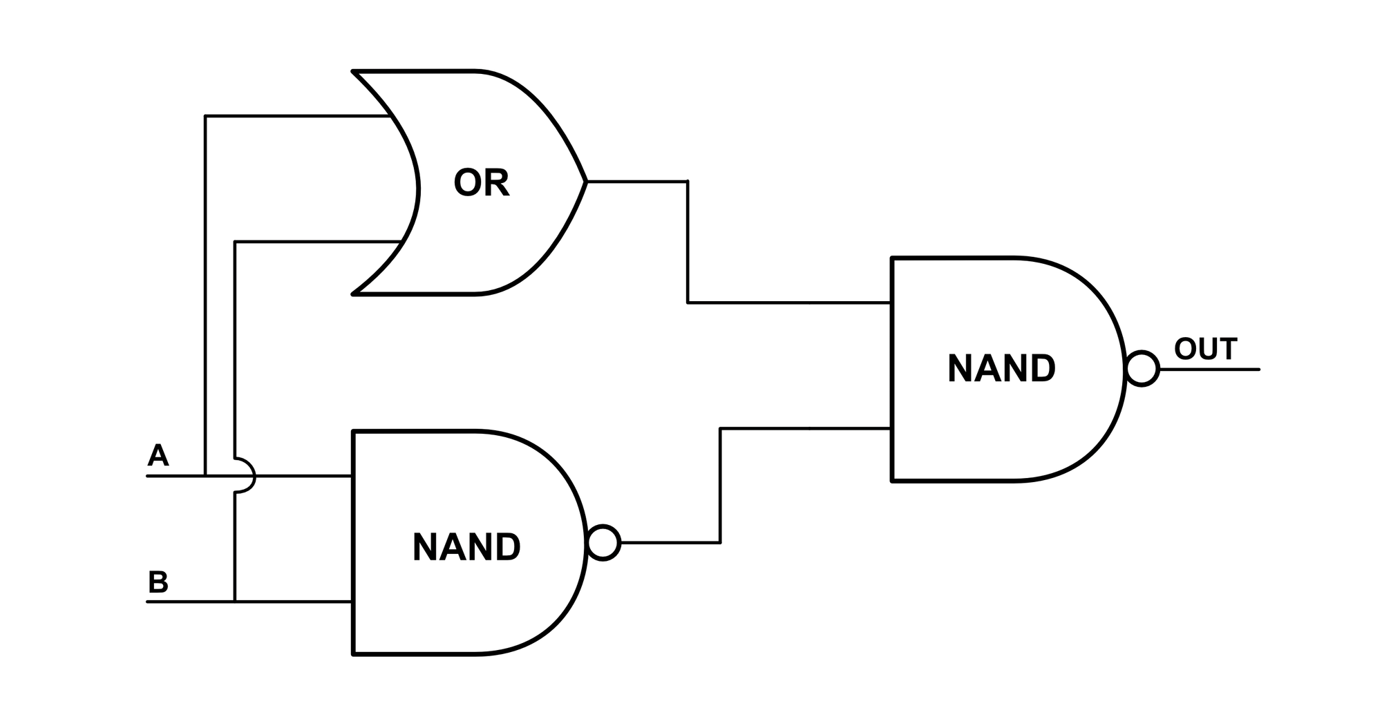
The XNOR gate is the exact opposite of the XOR gate. It can be constructed by replacing the XOR's AND gate with a NAND gate.
The XNOR logic table is shown below:
| A | B | Output |
|---|---|---|
| 0 | 0 | 1 |
| 1 | 0 | 0 |
| 0 | 1 | 0 |
| 1 | 1 | 1 |
The XNOR gate symbol is shown below:
Other Possible Gates
Discounting the NOT gate, which only has one input, we've so far discussed six different kinds of two input logic gates; AND, OR, NAND, NOR, XOR, and XNOR. If we consider all possible combinations, there are 16 possible different logic combinations for any gate with 2 inputs and one output.
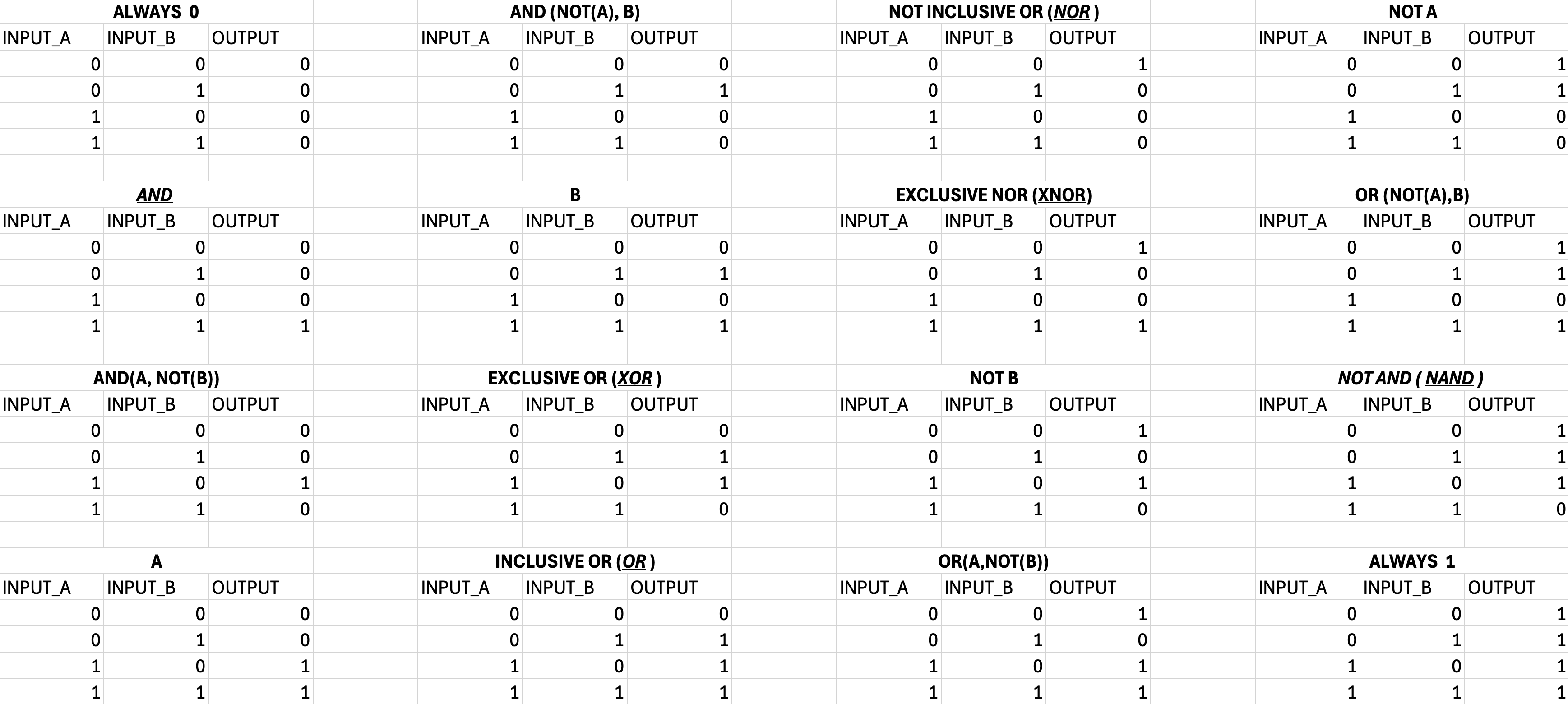
Some of these gates aren't very useful. For example, there isn't a clear reason why we would ever use an ALWAYS 0 or ALWAYS 1 gate. The two input A, B, NOT A, and NOT B gates are also rather silly since one of the inputs is always unused. This leaves us with 10 actually useful gates, six of which we have special names for and the rest of which can be created directly from switches or from a composition of gates (like NAND or NOR). For example, the AND(NOT(A),B) gate can be made from either discrete switches or gates:
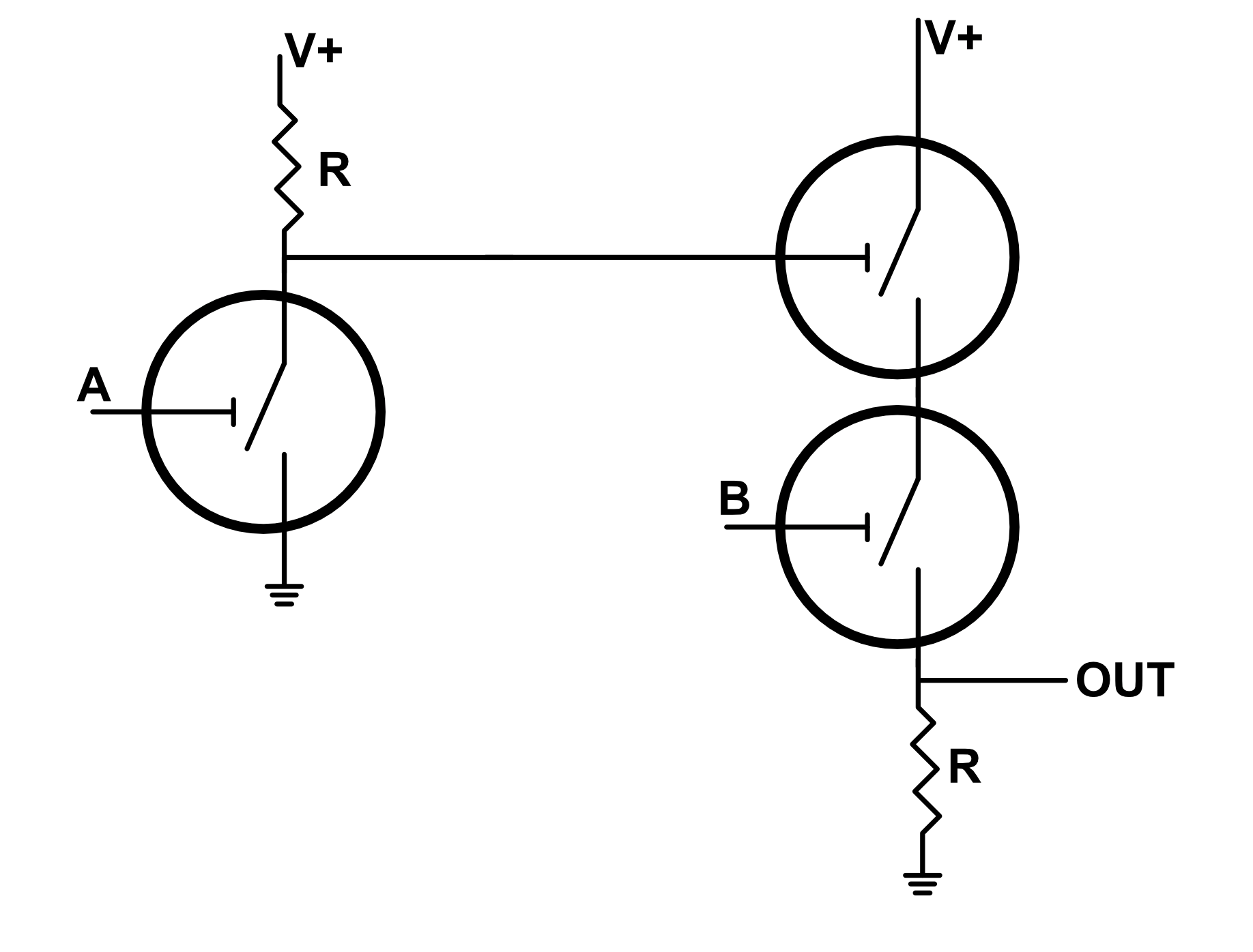
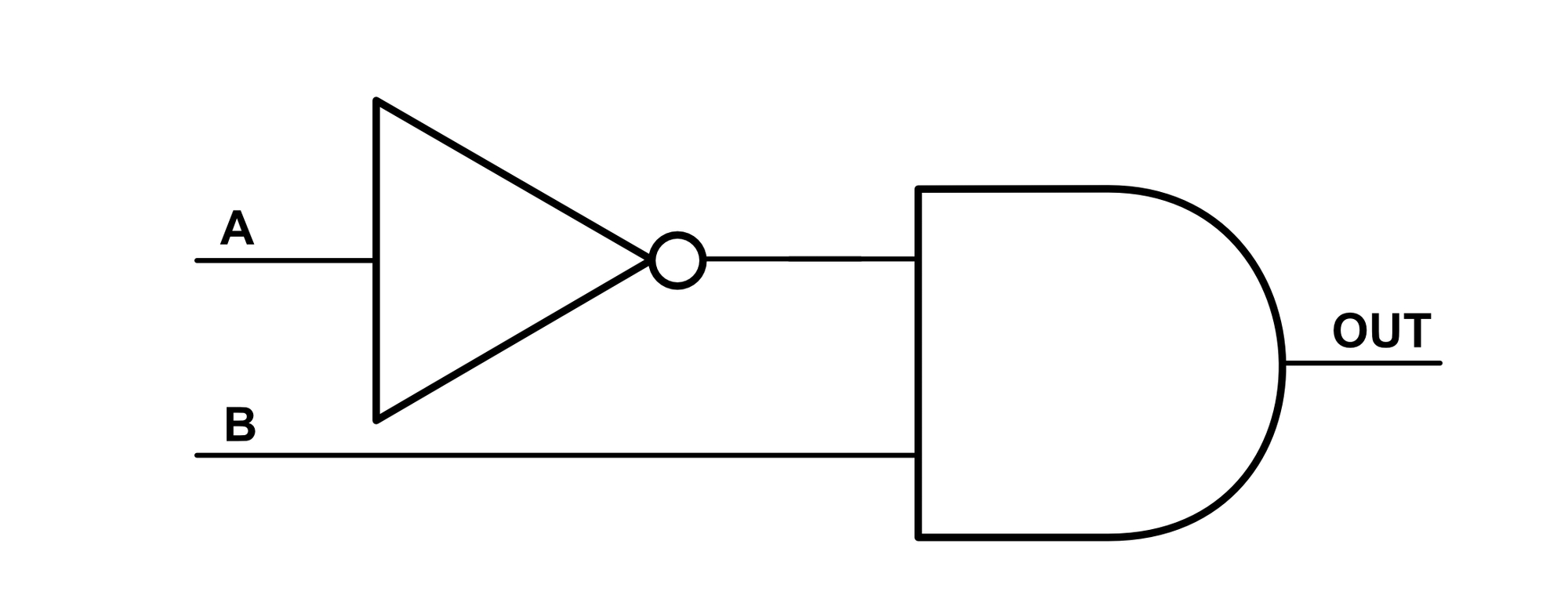
Figure 18: Left- Arrangement of switches for AND(NOT(A),B) gate | Right- Arrangement of logic gates for AND(NOT(A),B) gate
The fact that there are only 16 possible gates may at first appear limiting, but it's actually very liberating. There are infinitely many different methods of combining switches or logic gates into a two input single output device, yet no matter how they are combined, the resulting device will conform exactly to one of the 16 possible gate types.
Once we have constructed the simplest possible gate of each type, there is no more work to be done at the gate design level. We can stack gates to form increasingly complex devices while optimizing to reduce the total number of required gates. For a given logic device, there is actually an optimal hardware design solution (though modern devices are so complicated it isn't often practical to solve for it).
Multi-Input Logic Gates
Basic logic gates only have two inputs, but by stacking logic gates, we can obtain gates with more than two inputs. Below is a diagram and logic table for a 3 input AND gate:
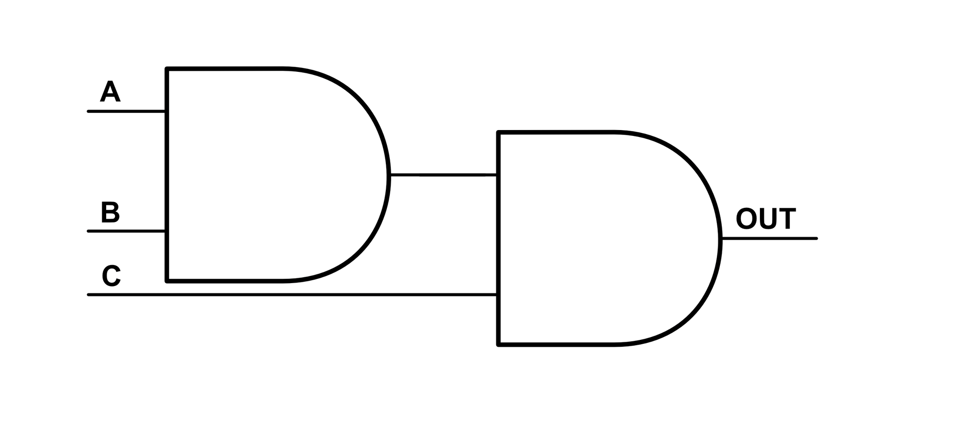
| A | B | C | Output |
|---|---|---|---|
| 0 | 0 | 0 | 0 |
| 0 | 0 | 1 | 0 |
| 0 | 1 | 0 | 0 |
| 0 | 1 | 1 | 0 |
| 1 | 0 | 0 | 0 |
| 1 | 0 | 1 | 0 |
| 1 | 1 | 0 | 0 |
| 1 | 1 | 1 | 1 |
Below is a diagram and logic table for a 3 input OR gate:
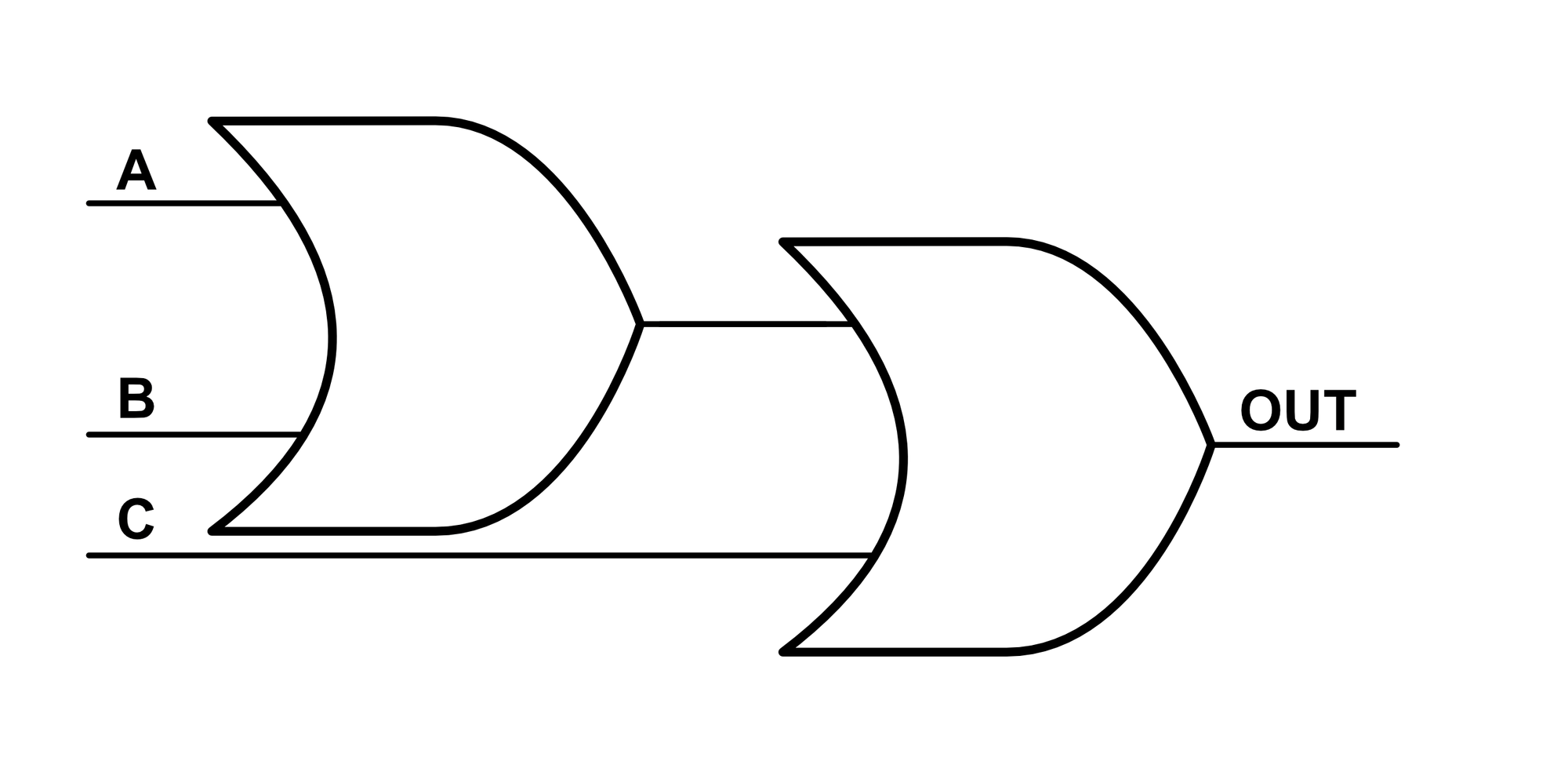
| A | B | C | Output |
|---|---|---|---|
| 0 | 0 | 0 | 0 |
| 0 | 0 | 1 | 1 |
| 0 | 1 | 0 | 1 |
| 0 | 1 | 1 | 1 |
| 1 | 0 | 0 | 1 |
| 1 | 0 | 1 | 1 |
| 1 | 1 | 0 | 1 |
| 1 | 1 | 1 | 1 |
There are many other multi-input gates that can be constructed, but mapping all possible combinations is well beyond the scope of this article.
